参数资料
| 型号: | AT25020AY1-10YU-1.8 |
| 厂商: | Atmel |
| 文件页数: | 8/22页 |
| 文件大小: | 0K |
| 描述: | IC EEPROM 2KBIT 20MHZ 8MAP |
| 标准包装: | 120 |
| 格式 - 存储器: | EEPROMs - 串行 |
| 存储器类型: | EEPROM |
| 存储容量: | 2K (256 x 8) |
| 速度: | 5MHz,10MHz,20MHz |
| 接口: | SPI 3 线串行 |
| 电源电压: | 1.8 V ~ 5.5 V |
| 工作温度: | -40°C ~ 85°C |
| 封装/外壳: | 8-UDFN 裸露焊盘 |
| 供应商设备封装: | 8-MAP(3x4.9) |
| 包装: | 管件 |
| 产品目录页面: | 1456 (CN2011-ZH PDF) |
| 其它名称: | AT25020AY110YU1.8 |
�� �
�
�Functional�
�Description�
�The� AT25010A/020A/040A� is� designed� to� interface� directly� with� the� synchronous� serial�
�peripheral� interface� (SPI)� of� the� 6805� and� 68HC11� series� of� microcontrollers.�
�The� AT25010A/020A/040A� utilizes� an� 8-bit� instruction� register.� The� list� of� instructions�
�and� their� operation� codes� are� contained� in� Figure� 5.� All� instructions,� addresses,� and�
�data� are� transferred� with� the� MSB� first� and� start� with� a� high-to-low� CS� transition.�
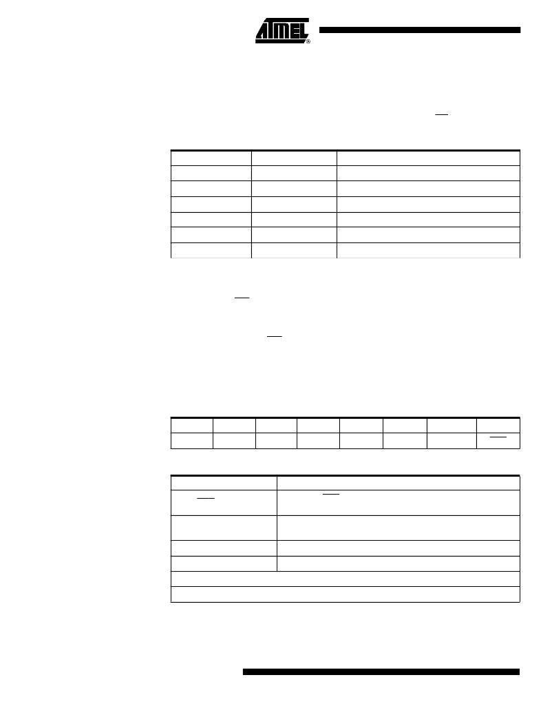
�Table� 5.� Instruction� Set� for� the� AT25010A/020A/040A�
�Instruction� Name�
�WREN�
�WRDI�
�RDSR�
�WRSR�
�READ�
�WRITE�
�Instruction� Format�
�0000� X110�
�0000� X100�
�0000� X101�
�0000� X001�
�0000� A011�
�0000� A010�
�Operation�
�Set� Write� Enable� Latch�
�Reset� Write� Enable� Latch�
�Read� Status� Register�
�Write� Status� Register�
�Read� Data� from� Memory� Array�
�Write� Data� to� Memory� Array�
�Note:�
�“A”� represents� MSB� address� bit� A8.�
�WRITE� ENABLE� (WREN):� The� device� will� power� up� in� the� write� disable� state� when� V� CC�
�is� applied.� All� programming� instructions� must� therefore� be� preceded� by� a� Write� Enable�
�instruction.� The� WP� pin� must� be� held� high� during� a� WREN� instruction.�
�WRITE� DISABLE� (WRDI):� To� protect� the� device� against� inadvertent� writes,� the� Write�
�Disable� instruction� disables� all� programming� modes.� The� WRDI� instruction� is� indepen-�
�dent� of� the� status� of� the� WP� pin.�
�READ� STATUS� REGISTER� (RDSR):� The� Read� Status� Register� instruction� provides�
�access� to� the� status� register.� The� read/busy� and� write� enable� status� of� the� device� can�
�be� determined� by� the� RDSR� instruction.� Similarly,� the� block� write� protection� bits� indicate�
�the� extent� of� protection� employed.� These� bits� are� set� by� using� the� WRSR� instruction.�
�Table� 6.� Status� Register� Format�
�Bit� 7�
�X�
�Bit� 6�
�X�
�Bit� 5�
�X�
�Bit� 4�
�X�
�Bit� 3�
�BP1�
�Bit� 2�
�BP0�
�Bit� 1�
�WEN�
�Bit� 0�
�RDY�
�Table� 7.� Read� Status� Register� Bit� Definition�
�Bit�
�Bit� 0� (RDY)�
�Bit� 1� (WEN)�
�Bit� 2� (BP0)�
�Bit� 3� (BP1)�
�Definition�
�Bit� 0� =� “0”� (RDY)� indicates� the� device� is� ready.� Bit� 0� =� “1”�
�indicates� the� write� cycle� is� in� progress.�
�Bit� 1� =� “0”� indicates� the� device� is� not� write� enabled.� Bit� 1� =� “1”�
�indicates� the� device� is� write� enabled.�
�See� Table� 8.�
�See� Table� 8.�
�Bits� 4–7� are� “0”s� when� device� is� not� in� an� internal� write� cycle.�
�Bits� 0–7� are� “1”s� during� an� internal� write� cycle.�
�WRITE� STATUS� REGISTER� (WRSR):� The� WRSR� instruction� allows� the� user� to� select�
�one� of� four� levels� of� protection.� The� AT25010A/020A/040A� is� divided� into� four� array� seg-�
�ments.� One-quarter,� one-half,� or� all� of� the� memory� segments� can� be� protected.� Any� of�
�8�
�AT25010A/020A/040A�
�3348J–SEEPR–8/06�
�相关PDF资料 |
PDF描述 |
|---|---|
| A3PN250-ZVQ100I | IC FPGA NANO 250K GATES 100-VQFP |
| ACC44DREN-S734 | CONN EDGECARD 88POS .100 EYELET |
| A3P125-1VQ100I | IC FPGA 1KB FLASH 125K 100-VQFP |
| AT93C46E-TH-B | IC EEPROM 1KBIT 2MHZ 8TSSOP |
| A3P125-1VQG100I | IC FPGA 1KB FLASH 125K 100-VQFP |
相关代理商/技术参数 |
参数描述 |
|---|---|
| AT25020AY6-10YH-1.8 | 功能描述:电可擦除可编程只读存储器 PB/HALO FREE, 1.8V RoHS:否 制造商:Atmel 存储容量:2 Kbit 组织:256 B x 8 数据保留:100 yr 最大时钟频率:1000 KHz 最大工作电流:6 uA 工作电源电压:1.7 V to 5.5 V 最大工作温度:+ 85 C 安装风格:SMD/SMT 封装 / 箱体:SOIC-8 |
| AT25020B | 制造商:ATMEL 制造商全称:ATMEL Corporation 功能描述:f serial electrically erasable able programmable read-only memory |
| AT25020B-MAHL-T | 功能描述:电可擦除可编程只读存储器 2K (256 X 8) SPI, 1.8V RoHS:否 制造商:Atmel 存储容量:2 Kbit 组织:256 B x 8 数据保留:100 yr 最大时钟频率:1000 KHz 最大工作电流:6 uA 工作电源电压:1.7 V to 5.5 V 最大工作温度:+ 85 C 安装风格:SMD/SMT 封装 / 箱体:SOIC-8 |
| AT25020B-SSHL-B | 功能描述:电可擦除可编程只读存储器 2K (256 X 8) SPI, 1.8V RoHS:否 制造商:Atmel 存储容量:2 Kbit 组织:256 B x 8 数据保留:100 yr 最大时钟频率:1000 KHz 最大工作电流:6 uA 工作电源电压:1.7 V to 5.5 V 最大工作温度:+ 85 C 安装风格:SMD/SMT 封装 / 箱体:SOIC-8 |
| AT25020B-SSHL-T | 功能描述:电可擦除可编程只读存储器 2K (256 X 8) SPI, 1.8V RoHS:否 制造商:Atmel 存储容量:2 Kbit 组织:256 B x 8 数据保留:100 yr 最大时钟频率:1000 KHz 最大工作电流:6 uA 工作电源电压:1.7 V to 5.5 V 最大工作温度:+ 85 C 安装风格:SMD/SMT 封装 / 箱体:SOIC-8 |
发布紧急采购,3分钟左右您将得到回复。