- 您现在的位置:买卖IC网 > PDF目录381452 > AT45D081-RI (ATMEL CORP) 8-Megabit 5-volt Only Serial DataFlash PDF资料下载
参数资料
| 型号: | AT45D081-RI |
| 厂商: | ATMEL CORP |
| 元件分类: | DRAM |
| 英文描述: | 8-Megabit 5-volt Only Serial DataFlash |
| 中文描述: | 1M X 8 FLASH 5V PROM, PDSO28 |
| 封装: | 0.330 INCH, PLASTIC, SOIC-28 |
| 文件页数: | 2/16页 |
| 文件大小: | 115K |
| 代理商: | AT45D081-RI |
AT45D081
2
Device Operation
The device operation is controlled by instructions from the
host processor. The list of instructions and their associated
opcodes are contained in Tables 1 and 2. A valid instruc-
tion starts with the falling edge of CS followed by the appro-
priate 8-bit opcode and the desired buffer or main memory
address location. While the CS pin is low, toggling the SCK
pin controls the loading of the opcode and the desired
buffer or main memory address location through the SI
(serial input) pin. All instructions, addresses, and data are
transferred with the most significant bit (MSB) first.
Read
By specifying the appropriate opcode, data can be read
from the main memory or from either one of the two data
buffers.
MAIN MEMORY PAGE READ:
A main memory read allows
the user to read data directly from any one of the 4096
pages in the main memory, bypassing both of the data buff-
ers and leaving the contents of the buffers unchanged. To
start a page read, the 8-bit opcode, 52H, is followed by 24
address bits and 32 don’t care bits. In the AT45D081, the
first three address bits are reserved for larger density
devices (see Notes on page 7), the next 12 address bits
(PA11-PA0) specify the page address, and the next nine
address bits (BA8-BA0) specify the starting byte address
within the page. The 32 don’t care bits which follow the 24
address bits are sent to initialize the read operation. Fol-
lowing the 32 don’t care bits, additional pulses on SCK
result in serial data being output on the SO (serial output)
pin. The CS pin must remain low during the loading of the
opcode, the address bits, and the reading of data. When
the end of a page in main memory is reached during a main
memory page read, the device will continue reading at the
beginning of the same page. A low to high transition on the
CS pin will terminate the read operation and tri-state the
SO pin.
BUFFER READ:
Data can be read from either one of the
two buffers, using different opcodes to specify which buffer
to read from. An opcode of 54H is used to read data from
buffer 1, and an opcode of 56H is used to read data from
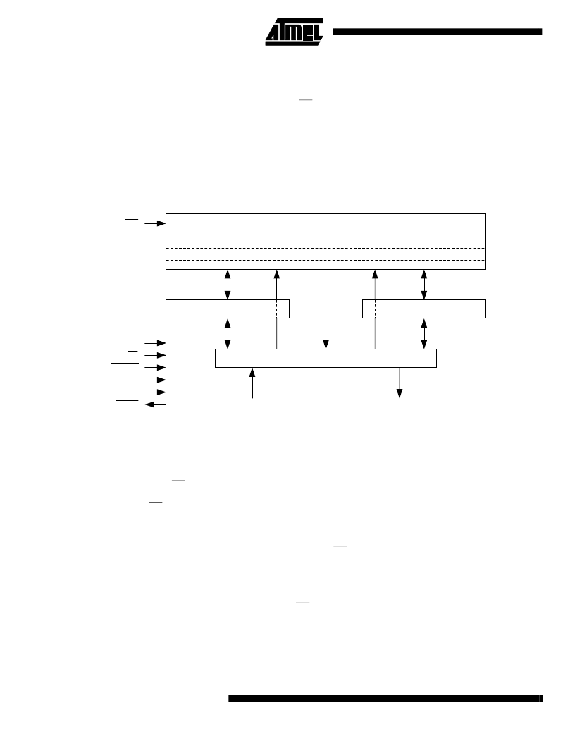
Block Diagram
FLASH MEMORY ARRAY
PAGE (264 BYTES)
BUFFER 2 (264 BYTES)
BUFFER 1 (264 BYTES)
I/O INTERFACE
SCK
CS
RESET
V
CC
GND
RDY/BUSY
WP
SO
SI
reduces package size and active pin count. The device is
optimized for use in many commercial and industrial appli-
cations where high density, low pin count, low voltage, and
low power are essential. Typical applications for the
DataFlash are digital voice storage, image storage, and
data storage. The device operates at clock frequencies up
to 10 Mhz with a typical active read current consumption of
15 mA.
To allow for simple in-system reprogrammability, the
AT45D081 does not require high input voltages for pro-
gramming. The device operates from a single power sup-
ply, 4.5V to 5.5V, for both the program and read opera-
tions. The AT45D081 is enabled through the chip select pin
(CS) and accessed via a three-wire interface consisting of
the Serial Input (SI), Serial Output (SO), and the Serial
Clock (SCK).
All programming cycles are self-timed, and no separate
erase cycle is required before programming.
相关PDF资料 |
PDF描述 |
|---|---|
| AT45D081-TC | 8-Megabit 5-volt Only Serial DataFlash |
| AT45D081-TI | 8-Megabit 5-volt Only Serial DataFlash |
| AT45D161-JC | 16-Megabit 5-volt Only Serial DataFlash |
| AT45D161-JI | 16-Megabit 5-volt Only Serial DataFlash |
| AT45D161-RC | 16-Megabit 5-volt Only Serial DataFlash |
相关代理商/技术参数 |
参数描述 |
|---|---|
| AT45D081-TC | 制造商:ATMEL 制造商全称:ATMEL Corporation 功能描述:8-Megabit 5-volt Only Serial DataFlash |
| AT45D081-TI | 制造商:ATMEL 制造商全称:ATMEL Corporation 功能描述:8-Megabit 5-volt Only Serial DataFlash |
| AT45D161 | 制造商:ATMEL 制造商全称:ATMEL Corporation 功能描述:16-megabit 5-volt Only Serial DataFlasH |
| AT45D161_01 | 制造商:ATMEL 制造商全称:ATMEL Corporation 功能描述:16-megabit 5-volt Only Serial DataFlasH |
| AT45D161-JC | 功能描述:闪存 16M bit RoHS:否 制造商:ON Semiconductor 数据总线宽度:1 bit 存储类型:Flash 存储容量:2 MB 结构:256 K x 8 定时类型: 接口类型:SPI 访问时间: 电源电压-最大:3.6 V 电源电压-最小:2.3 V 最大工作电流:15 mA 工作温度:- 40 C to + 85 C 安装风格:SMD/SMT 封装 / 箱体: 封装:Reel |
发布紧急采购,3分钟左右您将得到回复。