- 您现在的位置:买卖IC网 > PDF目录381453 > AT45DB021B-SC (ATMEL CORP) 2-megabit 2.7-volt Only DataFlash?? PDF资料下载
参数资料
| 型号: | AT45DB021B-SC |
| 厂商: | ATMEL CORP |
| 元件分类: | DRAM |
| 英文描述: | 2-megabit 2.7-volt Only DataFlash?? |
| 中文描述: | 2M X 1 FLASH 2.7V PROM, PDSO8 |
| 封装: | 0.209 INCH, PLASTIC, EIAJ, SOIC-8 |
| 文件页数: | 2/33页 |
| 文件大小: | 261K |
| 代理商: | AT45DB021B-SC |
第1页当前第2页第3页第4页第5页第6页第7页第8页第9页第10页第11页第12页第13页第14页第15页第16页第17页第18页第19页第20页第21页第22页第23页第24页第25页第26页第27页第28页第29页第30页第31页第32页第33页
2
AT45DB021B
1937F
–
DFLSH
–
10/02
EEPROM emulation (bit or byte alterability) is easily handled with a self-contained three
step Read-Modify-Write operation. Unlike conventional Flash memories that are
accessed randomly with multiple address lines and a parallel interface, the DataFlash
uses a SPI serial interface to sequentially access its data. DataFlash supports SPI mode
0 and mode 3. The simple serial interface facilitates hardware layout, increases system
reliability, minimizes switching noise, and reduces package size and active pin count.
The device is optimized for use in many commercial and industrial applications where
high density, low pin count, low voltage, and low power are essential. The device oper-
ates at clock frequencies up to 20 MHz with a typical active read current consumption of
4 mA.
To allow for simple in-system reprogrammability, the AT45DB021B does not require
high input voltages for programming. The device operates from a single power supply,
2.7V to 3.6V, for both the program and read operations. The AT45DB021B is enabled
through the chip select pin (CS) and accessed via a three-wire interface consisting of
the Serial Input (SI), Serial Output (SO), and the Serial Clock (SCK).
All programming cycles are self-timed, and no separate erase cycle is required before
programming.
When the device is shipped from Atmel, the most significant page of the memory array
may not be erased. In other words, the contents of the last page may not be filled with
FFH.
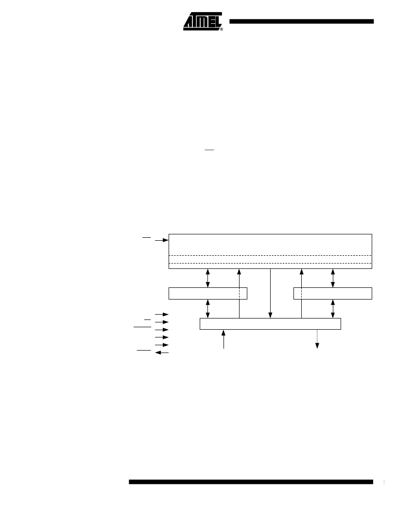
Block Diagram
Memory Array
To provide optimal flexibility, the memory array of the AT45DB021B is divided into three
levels of granularity comprised of sectors, blocks and pages. The Memory Architecture
Diagram illustrates the breakdown of each level and details the number of pages per
sector and block. All program operations to the DataFlash occur on a page-by-page
basis; however, the optional erase operations can be performed at the block or page
level.
FLASH MEMORY ARRAY
PAGE (264 BYTES)
BUFFER 2 (264 BYTES)
BUFFER 1 (264 BYTES)
I/O INTERFACE
SCK
CS
RESET
VCC
GND
RDY/BUSY
WP
SO
SI
相关PDF资料 |
PDF描述 |
|---|---|
| AT45DB021B-CC | 2-megabit 2.7-volt Only DataFlash?? |
| AT45DB021B-CI | 2-megabit 2.7-volt Only DataFlash?? |
| AT45DB021B-RC | 2-megabit 2.7-volt Only DataFlash?? |
| AT45DB021B-RI | 2-megabit 2.7-volt Only DataFlash?? |
| AT45DB021B-SI | 2-megabit 2.7-volt Only DataFlash?? |
相关代理商/技术参数 |
参数描述 |
|---|---|
| AT45DB021B-SI | 功能描述:闪存 2M bit RoHS:否 制造商:ON Semiconductor 数据总线宽度:1 bit 存储类型:Flash 存储容量:2 MB 结构:256 K x 8 定时类型: 接口类型:SPI 访问时间: 电源电压-最大:3.6 V 电源电压-最小:2.3 V 最大工作电流:15 mA 工作温度:- 40 C to + 85 C 安装风格:SMD/SMT 封装 / 箱体: 封装:Reel |
| AT45DB021B-SU | 功能描述:闪存 2M 8 I/O Pins SPI 264B 2.7V RoHS:否 制造商:ON Semiconductor 数据总线宽度:1 bit 存储类型:Flash 存储容量:2 MB 结构:256 K x 8 定时类型: 接口类型:SPI 访问时间: 电源电压-最大:3.6 V 电源电压-最小:2.3 V 最大工作电流:15 mA 工作温度:- 40 C to + 85 C 安装风格:SMD/SMT 封装 / 箱体: 封装:Reel |
| AT45DB021B-TC | 功能描述:闪存 2M bit RoHS:否 制造商:ON Semiconductor 数据总线宽度:1 bit 存储类型:Flash 存储容量:2 MB 结构:256 K x 8 定时类型: 接口类型:SPI 访问时间: 电源电压-最大:3.6 V 电源电压-最小:2.3 V 最大工作电流:15 mA 工作温度:- 40 C to + 85 C 安装风格:SMD/SMT 封装 / 箱体: 封装:Reel |
| AT45DB021BTI | 制造商:Atmel Corporation 功能描述: |
| AT45DB021B-TI | 功能描述:闪存 2M 2.7V RoHS:否 制造商:ON Semiconductor 数据总线宽度:1 bit 存储类型:Flash 存储容量:2 MB 结构:256 K x 8 定时类型: 接口类型:SPI 访问时间: 电源电压-最大:3.6 V 电源电压-最小:2.3 V 最大工作电流:15 mA 工作温度:- 40 C to + 85 C 安装风格:SMD/SMT 封装 / 箱体: 封装:Reel |
发布紧急采购,3分钟左右您将得到回复。