- 您现在的位置:买卖IC网 > PDF目录381453 > AT45DB021D (Atmel Corp.) 2-megabit 2.7-volt DataFlash PDF资料下载
参数资料
| 型号: | AT45DB021D |
| 厂商: | Atmel Corp. |
| 英文描述: | 2-megabit 2.7-volt DataFlash |
| 中文描述: | 2兆位2.7伏的DataFlash |
| 文件页数: | 16/52页 |
| 文件大小: | 1108K |
| 代理商: | AT45DB021D |
第1页第2页第3页第4页第5页第6页第7页第8页第9页第10页第11页第12页第13页第14页第15页当前第16页第17页第18页第19页第20页第21页第22页第23页第24页第25页第26页第27页第28页第29页第30页第31页第32页第33页第34页第35页第36页第37页第38页第39页第40页第41页第42页第43页第44页第45页第46页第47页第48页第49页第50页第51页第52页
16
3638B–DFLASH–02/07
AT45DB021D [Preliminary]
9.1.2
Program Sector Protection Register Command
Once the Sector Protection Register has been erased, it can be reprogrammed using the
Program Sector Protection Register command.
To program the Sector Protection Register, the CS pin must first be asserted and the appropri-
ate 4-byte opcode sequence must be clocked into the device via the SI pin. The 4-byte opcode
sequence must start with 3DH and be followed by 2AH, 7FH, and FCH. After the last bit of the
opcode sequence has been clocked into the device, the data for the contents of the Sector Pro-
tection Register must be clocked in. As described in
Section 9.1
, the Sector Protection Register
contains 4 bytes of data, so 4 bytes must be clocked into the device. The first byte of data corre-
sponds to sector 0, the second byte corresponds to sector 1, the third byte corresponds to sector
2, and the last byte of data corresponding to sector 3.
After the last data byte has been clocked in, the CS pin must be deasserted to initiate the inter-
nally self-timed program cycle. The programming of the Sector Protection Register should take
place in a time of t
P
, during which time the Status Register will indicate that the device is busy. If
the device is powered-down during the program cycle, then the contents of the Sector Protection
Register cannot be guaranteed.
If the proper number of data bytes is not clocked in before the CS pin is deasserted, then the
protection status of the sectors corresponding to the bytes not clocked in can not be guaranteed.
For example, if only the first two bytes are clocked in instead of the complete 4 bytes, then the
protection status of the last 2 sectors cannot be guaranteed. Furthermore, if more than 4 bytes
of data is clocked into the device, then the data will wrap back around to the beginning of the
register. For instance, if 5 bytes of data are clocked in, then the 5th byte will be stored at byte
location 0 of the Sector Protection Register.
If a value other than 00H or FFH is clocked into a byte location of the Sector Protection Register,
then the protection status of the sector corresponding to that byte location cannot be guaran-
teed. For example, if a value of 17H is clocked into byte location 2 of the Sector Protection
Register, then the protection status of sector 2 cannot be guaranteed.
The Sector Protection Register can be reprogrammed while the sector protection enabled or dis-
abled. Being able to reprogram the Sector Protection Register with the sector protection enabled
allows the user to temporarily disable the sector protection to an individual sector rather than
disabling sector protection completely.
The Program Sector Protection Register command utilizes the internal SRAM buffer for
processing. Therefore, the contents of the buffer will be altered from its previous state when this
command is issued.
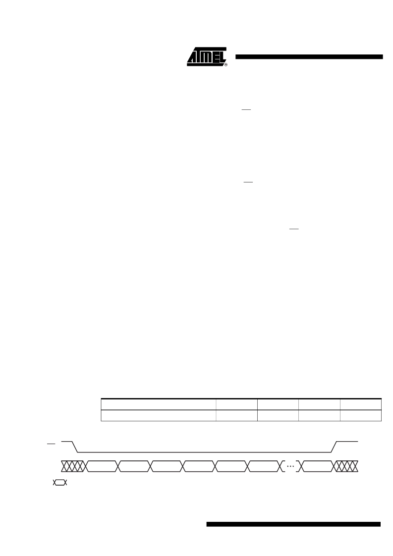
Figure 9-3.
Program Sector Protection Register
Command
Byte 1
Byte 2
Byte 3
Byte 4
Program Sector Protection Register
3DH
2AH
7FH
FCH
Data Byte
n
Opcode
Byte 1
Opcode
Byte 2
Opcode
Byte 3
Opcode
Byte 4
Data Byte
n + 1
Data Byte
n + 3
CS
Each transition
represents
8
b
its
SI
相关PDF资料 |
PDF描述 |
|---|---|
| AT45DB021D_07 | 2-megabit 2.7-volt DataFlash |
| AT45DB021D-MU | 2-megabit 2.7-volt DataFlash |
| AT45DB021D-SSU | 2-megabit 2.7-volt DataFlash |
| AT45DB021D-SU | 2-megabit 2.7-volt DataFlash |
| AT45DB021 | 2-Megabit 2.7-volt Only Serial DataFlash |
相关代理商/技术参数 |
参数描述 |
|---|---|
| AT45DB021D_07 | 制造商:ATMEL 制造商全称:ATMEL Corporation 功能描述:2-megabit 2.7-volt DataFlash |
| AT45DB021D_08 | 制造商:ATMEL 制造商全称:ATMEL Corporation 功能描述:2-megabit 2.7-volt Minimum DataFlash |
| AT45DB021D_09 | 制造商:ATMEL 制造商全称:ATMEL Corporation 功能描述:2-megabit 2.7-volt Minimum DataFlash |
| AT45DB021D-MH-SL954 | 制造商:Adesto Technologies Corporation 功能描述:8-UDFN (5X6), IND TEMP, 2.7V, TRAY, 256 BYTE PAGE - Trays |
| AT45DB021D-MH-SL955 | 制造商:Adesto Technologies Corporation 功能描述:8-UDFN (5X6), IND TEMP, 2.7V, T&R, 256 BYTE PAGE - Tape and Reel |
发布紧急采购,3分钟左右您将得到回复。