- 您现在的位置:买卖IC网 > PDF目录381453 > AT45DB041D (Atmel Corp.) 4-megabit 2.5-volt or 2.7-volt DataFlash PDF资料下载
参数资料
| 型号: | AT45DB041D |
| 厂商: | Atmel Corp. |
| 英文描述: | 4-megabit 2.5-volt or 2.7-volt DataFlash |
| 中文描述: | 4兆位2.5伏或2.7伏的DataFlash |
| 文件页数: | 17/53页 |
| 文件大小: | 1085K |
| 代理商: | AT45DB041D |
第1页第2页第3页第4页第5页第6页第7页第8页第9页第10页第11页第12页第13页第14页第15页第16页当前第17页第18页第19页第20页第21页第22页第23页第24页第25页第26页第27页第28页第29页第30页第31页第32页第33页第34页第35页第36页第37页第38页第39页第40页第41页第42页第43页第44页第45页第46页第47页第48页第49页第50页第51页第52页第53页
17
3595H–DFLASH–03/07
AT45DB041D
9.1.3
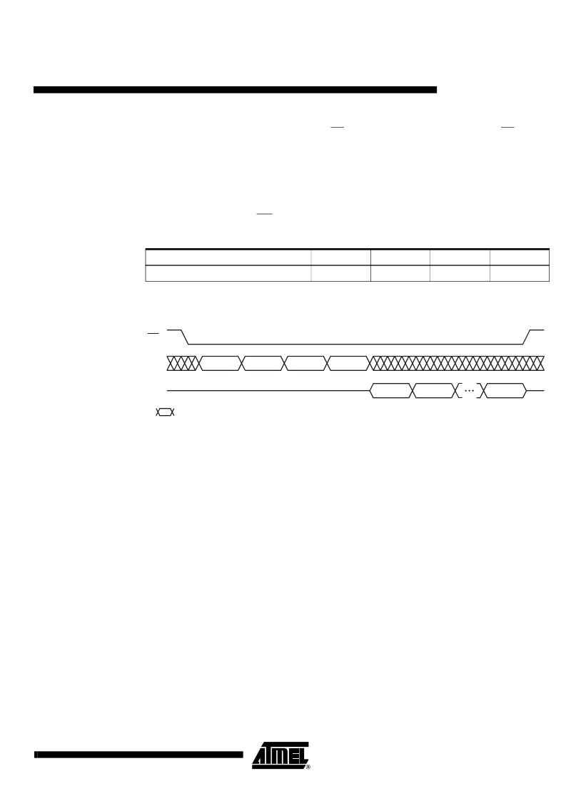
Read Sector Protection Register Command
To read the Sector Protection Register, the CS pin must first be asserted. Once the CS pin has
been asserted, an opcode of 32H and 3 dummy bytes must be clocked in via the SI pin. After the
last bit of the opcode and dummy bytes have been clocked in, any additional clock pulses on the
SCK pins will result in data for the content of the Sector Protection Register being output on the
SO pin. The first byte corresponds to sector 0 (0a, 0b), the second byte corresponds to sector 1
and the last byte (byte 8) corresponds to sector 7. Once the last byte of the Sector Protection
Register has been clocked out, any additional clock pulses will result in undefined data being
output on the SO pin. The CS must be deasserted to terminate the Read Sector Protection Reg-
ister operation and put the output into a high-impedance state.
Note:
xx = Dummy Byte
Figure 9-4.
Read Sector Protection Register
9.1.4
Various Aspects About the Sector Protection Register
The Sector Protection Register is subject to a limit of 10,000 erase/program cycles. Users are
encouraged to carefully evaluate the number of times the Sector Protection Register will be
modified during the course of the applications’ life cycle. If the application requires that the Sec-
tor Protection Register be modified more than the specified limit of 10,000 cycles because the
application needs to temporarily unprotect individual sectors (sector protection remains enabled
while the Sector Protection Register is reprogrammed), then the application will need to limit this
practice. Instead, a combination of temporarily unprotecting individual sectors along with dis-
abling sector protection completely will need to be implemented by the application to ensure that
the limit of 10,000 cycles is not exceeded.
Command
Byte 1
Byte 2
Byte 3
Byte 4
Read Sector Protection Register
32H
xxH
xxH
xxH
Opcode
X
X
X
Data Byte
n
Data Byte
n + 1
CS
Data Byte
n + 7
SI
SO
Each transition
represents 8 bits
相关PDF资料 |
PDF描述 |
|---|---|
| AT45DB041D_07 | 4-megabit 2.5-volt or 2.7-volt DataFlash |
| AT45DB041D-MU | 4-megabit 2.5-volt or 2.7-volt DataFlash |
| AT45DB041D-MU-2.5 | 4-megabit 2.5-volt or 2.7-volt DataFlash |
| AT45DB041D-SSU | 4-megabit 2.5-volt or 2.7-volt DataFlash |
| AT45DB041D-SSU-2.5 | 4-megabit 2.5-volt or 2.7-volt DataFlash |
相关代理商/技术参数 |
参数描述 |
|---|---|
| AT45DB041D_07 | 制造商:ATMEL 制造商全称:ATMEL Corporation 功能描述:4-megabit 2.5-volt or 2.7-volt DataFlash |
| AT45DB041D_08 | 制造商:ATMEL 制造商全称:ATMEL Corporation 功能描述:4-megabit 2.5-volt or 2.7-volt DataFlash |
| AT45DB041D-DWF | 制造商:Adesto Technologies Corporation 功能描述:WHOLE WAFER, NO BACKGRIND - Gel-pak, waffle pack, wafer, diced wafer on film |
| AT45DB041D-MU | 功能描述:闪存 4MB SERIAL 2.5V - IND TEMP RoHS:否 制造商:ON Semiconductor 数据总线宽度:1 bit 存储类型:Flash 存储容量:2 MB 结构:256 K x 8 定时类型: 接口类型:SPI 访问时间: 电源电压-最大:3.6 V 电源电压-最小:2.3 V 最大工作电流:15 mA 工作温度:- 40 C to + 85 C 安装风格:SMD/SMT 封装 / 箱体: 封装:Reel |
| AT45DB041D-MU-2.5 | 功能描述:闪存 4MB SERIAL 2.5V - IND TEMP RoHS:否 制造商:ON Semiconductor 数据总线宽度:1 bit 存储类型:Flash 存储容量:2 MB 结构:256 K x 8 定时类型: 接口类型:SPI 访问时间: 电源电压-最大:3.6 V 电源电压-最小:2.3 V 最大工作电流:15 mA 工作温度:- 40 C to + 85 C 安装风格:SMD/SMT 封装 / 箱体: 封装:Reel |
发布紧急采购,3分钟左右您将得到回复。