- 您现在的位置:买卖IC网 > PDF目录381454 > AT45DB081B (Atmel Corp.) 8-megabit 2.5-volt Only or 2.7-volt Only DataFlash PDF资料下载
参数资料
| 型号: | AT45DB081B |
| 厂商: | Atmel Corp. |
| 英文描述: | 8-megabit 2.5-volt Only or 2.7-volt Only DataFlash |
| 中文描述: | 8兆位2.5伏或2.7只有伏只的DataFlash |
| 文件页数: | 5/32页 |
| 文件大小: | 414K |
| 代理商: | AT45DB081B |
第1页第2页第3页第4页当前第5页第6页第7页第8页第9页第10页第11页第12页第13页第14页第15页第16页第17页第18页第19页第20页第21页第22页第23页第24页第25页第26页第27页第28页第29页第30页第31页第32页
5
AT45DB081B
2225C
–
12/01
loaded into the device. After the last bit of the opcode is shifted in, the eight bits of the
status register, starting with the MSB (bit 7), will be shifted out on the SO pin during the
next eight clock cycles. The five most significant bits of the status register will contain
device information, while the remaining three least-significant bits are reserved for future
use and will have undefined values. After bit 0 of the status register has been shifted
out, the sequence will repeat itself (as long as CS remains low and SCK is being tog-
gled) starting again with bit 7. The data in the status register is constantly updated, so
each repeating sequence will output new data.
Ready/Busy status is indicated using bit 7 of the status register. If bit 7 is a 1, then the
device is not busy and is ready to accept the next command. If bit 7 is a 0, then the
device is in a busy state. The user can continuously poll bit 7 of the status register by
stopping SCK at a low level once bit 7 has been output. The status of bit 7 will continue
to be output on the SO pin, and once the device is no longer busy, the state of SO will
change from 0 to 1. There are eight operations which can cause the device to be in a
busy state: Main Memory Page to Buffer Transfer, Main Memory Page to Buffer Com-
pare, Buffer to Main Memory Page Program with Built-in Erase, Buffer to Main Memory
Page Program without Built-in Erase, Page Erase, Block Erase, Main Memory Page
Program, and Auto Page Rewrite.
The result of the most recent Main Memory Page to Buffer Compare operation is indi-
cated using bit 6 of the status register. If bit 6 is a 0, then the data in the main memory
page matches the data in the buffer. If bit 6 is a 1, then at least one bit of the data in the
main memory page does not match the data in the buffer.
The device density is indicated using bits 5, 4, and 3 of the status register. For the
AT45DB081B, the three bits are 1, 0, and 0. The decimal value of these three binary bits
does not equate to the device density; the three bits represent a combinational code
relating to differing densities of Serial DataFlash devices, allowing a total of eight differ-
ent density configurations.
Program and Erase
Commands
BUFFER WRITE:
Data can be shifted in from the SI pin into either buffer 1 or buffer 2.
To load data into either buffer, an 8-bit opcode, 84H for buffer 1 or 87H for buffer 2, must
be followed by 15 don
’
t care bits and nine address bits (BFA8 - BFA0). The nine
address bits specify the first byte in the buffer to be written. The data is entered following
the address bits. If the end of the data buffer is reached, the device will wrap around
back to the beginning of the buffer. Data will continue to be loaded into the buffer until a
low-to-high transition is detected on the CS pin.
BUFFER TO MAIN MEMORY PAGE PROGRAM WITH BUILT-IN ERASE:
Data written
into either buffer 1 or buffer 2 can be programmed into the main memory. To start the
operation, an 8-bit opcode, 83H for buffer 1 or 86H for buffer 2, must be followed by the
three reserved bits, 12 address bits (PA11 - PA0) that specify the page in the main
memory to be written, and nine additional don
’
t care bits. When a low-to-high transition
occurs on the CS pin, the part will first erase the selected page in main memory to all 1s
and then program the data stored in the buffer into the specified page in the main mem-
ory. Both the erase and the programming of the page are internally self-timed and
should take place in a maximum time of t
EP
. During this time, the status register will indi-
cate that the part is busy.
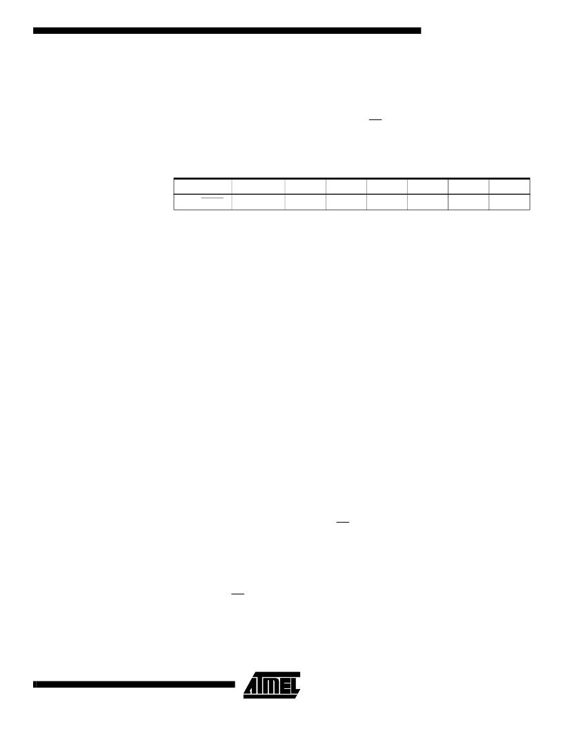
Status Register Format
Bit 7
Bit 6
Bit 5
Bit 4
Bit 3
Bit 2
Bit 1
Bit 0
RDY/BUSY
COMP
1
0
0
X
X
X
相关PDF资料 |
PDF描述 |
|---|---|
| AT45DB081B-CC-2.5 | SERIAL EEPROM|FLASH|4KX264X8|CMOS|BGA|14PIN|PLASTIC |
| AT45DB081B-RC-2.5 | SERIAL EEPROM|FLASH|4KX264X8|CMOS|SOP|28PIN|PLASTIC |
| AT45DB081B-TC | SERIAL EEPROM|FLASH|4KX264X8|CMOS|TSSOP|28PIN|PLASTIC |
| AT45DB081B-TC-2.5 | SERIAL EEPROM|FLASH|4KX264X8|CMOS|TSSOP|28PIN|PLASTIC |
| AT45DB081B-TI | SERIAL EEPROM|FLASH|4KX264X8|CMOS|TSSOP|28PIN|PLASTIC |
相关代理商/技术参数 |
参数描述 |
|---|---|
| AT-45DB081B | 制造商:ATMEL 制造商全称:ATMEL Corporation 功能描述:AT-45DB081B DATA FLASH RELIABILITY DATA |
| AT45DB081B_05 | 制造商:ATMEL 制造商全称:ATMEL Corporation 功能描述:8-megabit 2.5-volt Only or 2.7-volt Only DataFlash |
| AT45DB081B-CC | 功能描述:闪存 8M bit RoHS:否 制造商:ON Semiconductor 数据总线宽度:1 bit 存储类型:Flash 存储容量:2 MB 结构:256 K x 8 定时类型: 接口类型:SPI 访问时间: 电源电压-最大:3.6 V 电源电压-最小:2.3 V 最大工作电流:15 mA 工作温度:- 40 C to + 85 C 安装风格:SMD/SMT 封装 / 箱体: 封装:Reel |
| AT45DB081B-CC-2.5 | 功能描述:闪存 DATAFLASH 2M SERIAL 2.7V 2.5V COM TEMP RoHS:否 制造商:ON Semiconductor 数据总线宽度:1 bit 存储类型:Flash 存储容量:2 MB 结构:256 K x 8 定时类型: 接口类型:SPI 访问时间: 电源电压-最大:3.6 V 电源电压-最小:2.3 V 最大工作电流:15 mA 工作温度:- 40 C to + 85 C 安装风格:SMD/SMT 封装 / 箱体: 封装:Reel |
| AT45DB081B-CI | 功能描述:闪存 8M bit RoHS:否 制造商:ON Semiconductor 数据总线宽度:1 bit 存储类型:Flash 存储容量:2 MB 结构:256 K x 8 定时类型: 接口类型:SPI 访问时间: 电源电压-最大:3.6 V 电源电压-最小:2.3 V 最大工作电流:15 mA 工作温度:- 40 C to + 85 C 安装风格:SMD/SMT 封装 / 箱体: 封装:Reel |
发布紧急采购,3分钟左右您将得到回复。