- 您现在的位置:买卖IC网 > PDF目录381454 > AT45DB081D_07 (Atmel Corp.) 8-megabit 2.5-volt or 2.7-volt DataFlash PDF资料下载
参数资料
| 型号: | AT45DB081D_07 |
| 厂商: | Atmel Corp. |
| 英文描述: | 8-megabit 2.5-volt or 2.7-volt DataFlash |
| 中文描述: | 8兆位2.5伏或2.7伏的DataFlash |
| 文件页数: | 15/53页 |
| 文件大小: | 1105K |
| 代理商: | AT45DB081D_07 |
第1页第2页第3页第4页第5页第6页第7页第8页第9页第10页第11页第12页第13页第14页当前第15页第16页第17页第18页第19页第20页第21页第22页第23页第24页第25页第26页第27页第28页第29页第30页第31页第32页第33页第34页第35页第36页第37页第38页第39页第40页第41页第42页第43页第44页第45页第46页第47页第48页第49页第50页第51页第52页第53页
15
3596E–DFLASH–02/07
AT45DB081D
9.1.1
Erase Sector Protection Register Command
In order to modify and change the values of the Sector Protection Register, it must first be
erased using the Erase Sector Protection Register command.
To erase the Sector Protection Register, the CS pin must first be asserted as it would be with
any other command. Once the CS pin has been asserted, the appropriate 4-byte opcode
sequence must be clocked into the device via the SI pin. The 4-byte opcode sequence must
start with 3DH and be followed by 2AH, 7FH, and CFH. After the last bit of the opcode sequence
has been clocked in, the CS pin must be deasserted to initiate the internally self-timed erase
cycle. The erasing of the Sector Protection Register should take place in a time of t
PE
, during
which time the Status Register will indicate that the device is busy. If the device is powered-
down before the completion of the erase cycle, then the contents of the Sector Protection Regis-
ter cannot be guaranteed.
The Sector Protection Register can be erased with the sector protection enabled or disabled.
Since the erased state (FFH) of each byte in the Sector Protection Register is used to indicate
that a sector is specified for protection, leaving the sector protection enabled during the erasing
of the register allows the protection scheme to be more effective in the prevention of accidental
programming or erasing of the device. If for some reason an erroneous program or erase com-
mand is sent to the device immediately after erasing the Sector Protection Register and before
the register can be reprogrammed, then the erroneous program or erase command will not be
processed because all sectors would be protected.
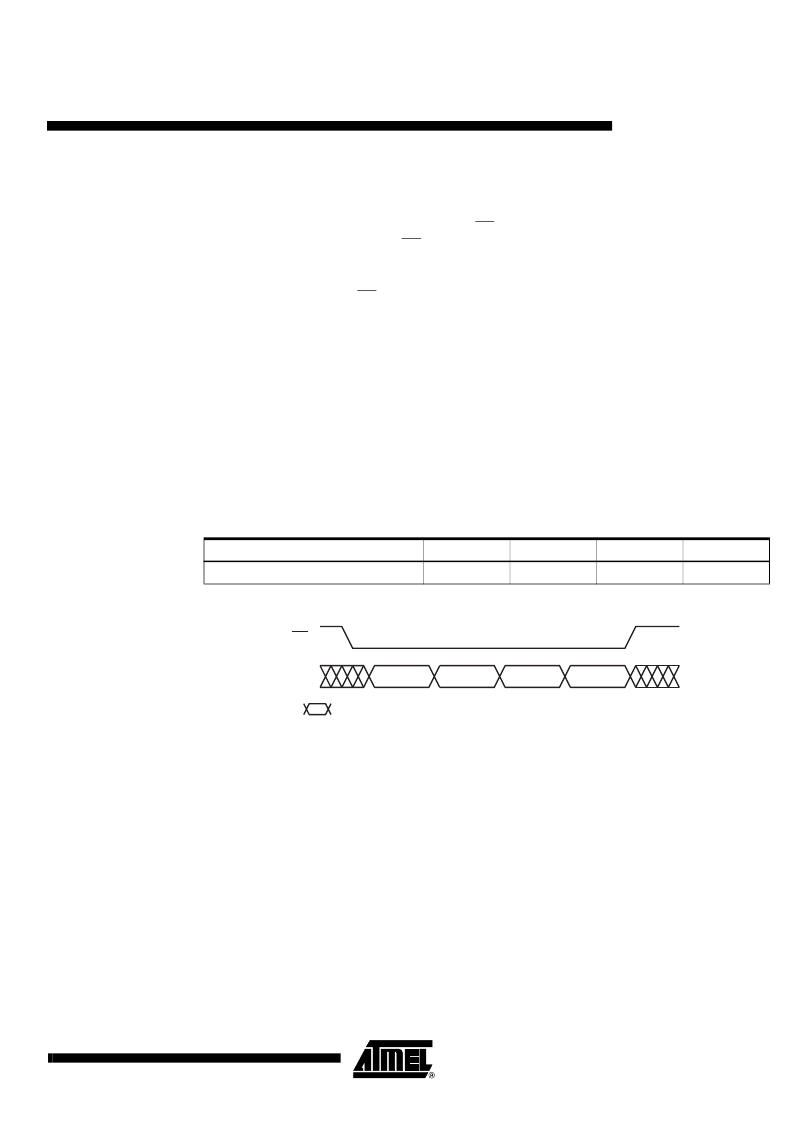
Figure 9-2.
Erase Sector Protection Register
Command
Byte 1
Byte 2
Byte 3
Byte 4
Erase Sector Protection Register
3DH
2AH
7FH
CFH
Opcode
Byte 1
Opcode
Byte 2
Opcode
Byte 3
Opcode
Byte 4
CS
Each transition
represents
8
b
its
SI
相关PDF资料 |
PDF描述 |
|---|---|
| AT45DB081D-MU | 8-megabit 2.5-volt or 2.7-volt DataFlash |
| AT45DB081D-MU-2.5 | 8-megabit 2.5-volt or 2.7-volt DataFlash |
| AT45DB081D-SSU | 8-megabit 2.5-volt or 2.7-volt DataFlash |
| AT45DB081D-SSU-2.5 | 8-megabit 2.5-volt or 2.7-volt DataFlash |
| AT45DB081D-SU | 8-megabit 2.5-volt or 2.7-volt DataFlash |
相关代理商/技术参数 |
参数描述 |
|---|---|
| AT45DB081D-DWF | 制造商:Adesto Technologies Corporation 功能描述:WHOLE WAFER, NO BACKGRIND - Gel-pak, waffle pack, wafer, diced wafer on film |
| AT45DB081D-MU | 功能描述:闪存 4M 2.7-3.6V 66Mhz Serial 闪存 RoHS:否 制造商:ON Semiconductor 数据总线宽度:1 bit 存储类型:Flash 存储容量:2 MB 结构:256 K x 8 定时类型: 接口类型:SPI 访问时间: 电源电压-最大:3.6 V 电源电压-最小:2.3 V 最大工作电流:15 mA 工作温度:- 40 C to + 85 C 安装风格:SMD/SMT 封装 / 箱体: 封装:Reel |
| AT45DB081D-MU SL383 | 制造商:Adesto Technologies Corporation 功能描述:DATAFLASH, 8MB, SERIAL, 2.7V - 2.5V, MLF, IND TEMP, GREEN PK - Tape and Reel |
| AT45DB081D-MU-2.5 | 功能描述:闪存 8MB SERIAL 2.5V - IND TEMP RoHS:否 制造商:ON Semiconductor 数据总线宽度:1 bit 存储类型:Flash 存储容量:2 MB 结构:256 K x 8 定时类型: 接口类型:SPI 访问时间: 电源电压-最大:3.6 V 电源电压-最小:2.3 V 最大工作电流:15 mA 工作温度:- 40 C to + 85 C 安装风格:SMD/SMT 封装 / 箱体: 封装:Reel |
| AT45DB081D-MU-2.5-SL383 | 制造商:Adesto Technologies Corporation 功能描述:8-VDFN (5X6), IND TEMP, 2.5V, T&R - Tape and Reel 制造商:Adesto Technologies Corporation 功能描述:IC FLASH 8MBIT 50MHZ 8VDFN |
发布紧急采购,3分钟左右您将得到回复。