- 您现在的位置:买卖IC网 > PDF目录381454 > AT45DB081D (Atmel Corp.) 8-megabit 2.5-volt or 2.7-volt DataFlash PDF资料下载
参数资料
| 型号: | AT45DB081D |
| 厂商: | Atmel Corp. |
| 英文描述: | 8-megabit 2.5-volt or 2.7-volt DataFlash |
| 中文描述: | 8兆位2.5伏或2.7伏的DataFlash |
| 文件页数: | 9/53页 |
| 文件大小: | 1105K |
| 代理商: | AT45DB081D |
第1页第2页第3页第4页第5页第6页第7页第8页当前第9页第10页第11页第12页第13页第14页第15页第16页第17页第18页第19页第20页第21页第22页第23页第24页第25页第26页第27页第28页第29页第30页第31页第32页第33页第34页第35页第36页第37页第38页第39页第40页第41页第42页第43页第44页第45页第46页第47页第48页第49页第50页第51页第52页第53页
9
3596E–DFLASH–02/07
AT45DB081D
7.4
Page Erase
The Page Erase command can be used to individually erase any page in the main memory array
allowing the Buffer to Main Memory Page Program to be utilized at a later time. To perform a
page erase in the DataFlash standard page size (264 bytes), an opcode of 81H must be loaded
into the device, followed by three address bytes comprised of 3 don’t care bits, 12 page address
bits (PA11 - PA0) that specify the page in the main memory to be erased and 9 don’t care bits.
To perform a page erase in the binary page size (256 bytes), the opcode 81H must be loaded
into the device, followed by three address bytes consist of 4 don’t care bits, 12 page address bits
(A19 - A8) that specify the page in the main memory to be erased and 8 don’t care bits.
W
hen a
low-to-high transition occurs on the CS pin, the part will erase the selected page (the erased
state is a logical 1). The erase operation is internally self-timed and should take place in a maxi-
mum time of t
PE
. During this time, the status register will indicate that the part is busy.
7.5
Block Erase
A block of eight pages can be erased at one time. This command is useful when large amounts
of data has to be written into the device. This will avoid using multiple Page Erase Commands.
To perform a block erase for the DataFlash standard page size (264 bytes), an opcode of 50H
must be loaded into the device, followed by three address bytes comprised of 3 don’t care bits,
9 page address bits (PA11 -PA3) and 12 don’t care bits. The 9 page address bits are used to
specify which block of eight pages is to be erased. To perform a block erase for the binary page
size (256 bytes), the opcode 50H must be loaded into the device, followed by three address
bytes consisting of 4 don’t care bits, 9 page address bits (A19 - A11) and 11 don’t care bits. The
9 page address bits are used to specify which block of eight pages is to be erased.
W
hen a low-
to-high transition occurs on the CS pin, the part will erase the selected block of eight pages. The
erase operation is internally self-timed and should take place in a maximum time of t
BE
. During
this time, the status register will indicate that the part is busy.
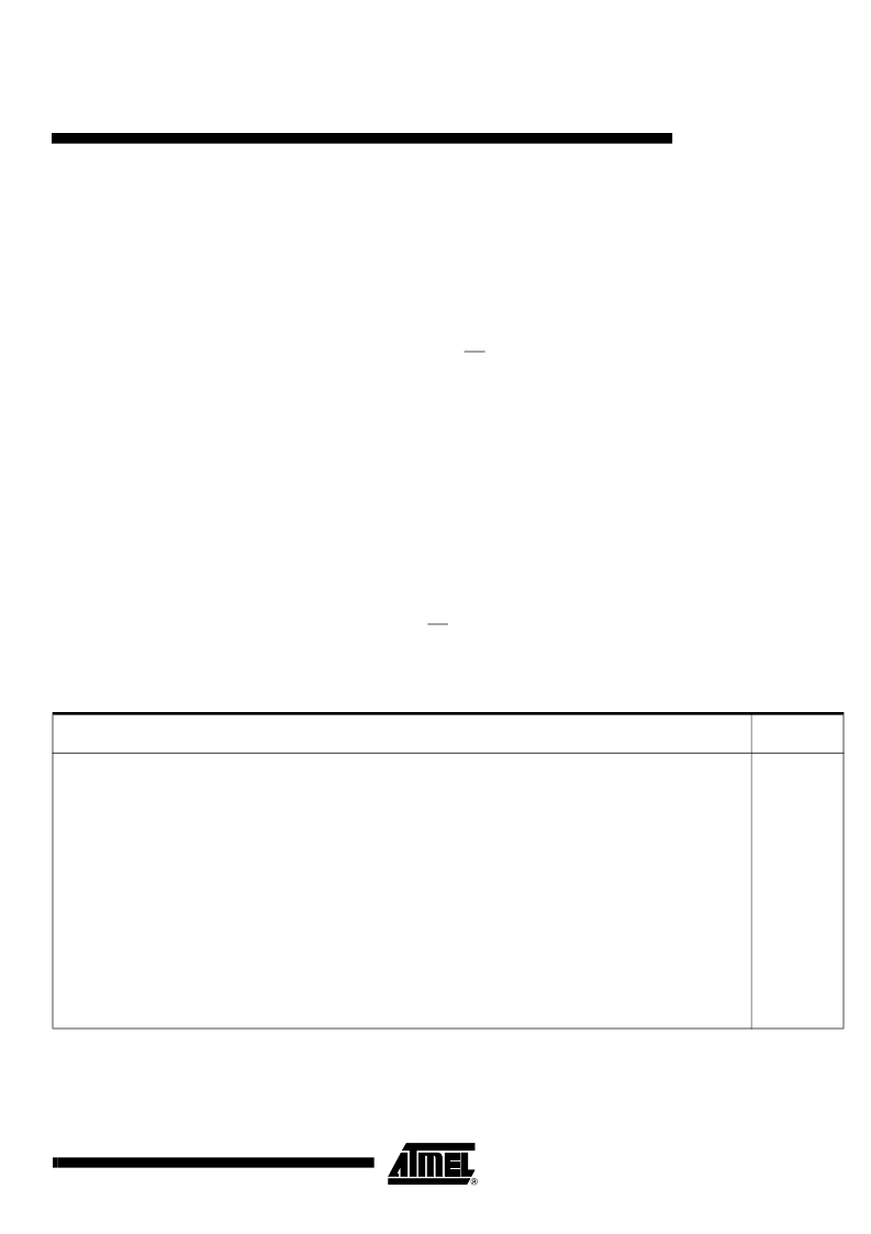
Table 7-1.
Block Erase Addressing
PA11/
A19
PA10/
A18
PA9/
A17
PA8/
A16
PA7/
A15
PA6/
A14
PA5/
A13
PA4/
A12
PA3/
A11
PA2/
A10
PA1/
A9
PA0/
A8
Block
0
0
0
0
0
0
0
0
0
X
X
X
0
0
0
0
0
0
0
0
0
1
X
X
X
1
0
0
0
0
0
0
0
1
0
X
X
X
2
0
0
0
0
0
0
0
1
1
X
X
X
3
1
1
1
1
1
1
1
0
0
X
X
X
508
1
1
1
1
1
1
1
0
1
X
X
X
509
1
1
1
1
1
1
1
1
0
X
X
X
510
1
1
1
1
1
1
1
1
1
X
X
X
511
相关PDF资料 |
PDF描述 |
|---|---|
| AT45DB081D_07 | 8-megabit 2.5-volt or 2.7-volt DataFlash |
| AT45DB081D-MU | 8-megabit 2.5-volt or 2.7-volt DataFlash |
| AT45DB081D-MU-2.5 | 8-megabit 2.5-volt or 2.7-volt DataFlash |
| AT45DB081D-SSU | 8-megabit 2.5-volt or 2.7-volt DataFlash |
| AT45DB081D-SSU-2.5 | 8-megabit 2.5-volt or 2.7-volt DataFlash |
相关代理商/技术参数 |
参数描述 |
|---|---|
| AT45DB081D_07 | 制造商:ATMEL 制造商全称:ATMEL Corporation 功能描述:8-megabit 2.5-volt or 2.7-volt DataFlash |
| AT45DB081D_08 | 制造商:ATMEL 制造商全称:ATMEL Corporation 功能描述:8-megabit 2.5-volt or 2.7-volt DataFlash |
| AT45DB081D_09 | 制造商:ATMEL 制造商全称:ATMEL Corporation 功能描述:8-megabit 2.5-volt or 2.7-volt DataFlash |
| AT45DB081D_13 | 制造商:AD 制造商全称:Analog Devices 功能描述:8-megabit 2.5V or 2.7V DataFlash |
| AT45DB081D-DWF | 制造商:Adesto Technologies Corporation 功能描述:WHOLE WAFER, NO BACKGRIND - Gel-pak, waffle pack, wafer, diced wafer on film |
发布紧急采购,3分钟左右您将得到回复。