- 您现在的位置:买卖IC网 > PDF目录20547 > AT45DB642-TI (Atmel)IC FLASH 64MBIT 20MHZ 40TSOP PDF资料下载
参数资料
| 型号: | AT45DB642-TI |
| 厂商: | Atmel |
| 文件页数: | 2/37页 |
| 文件大小: | 0K |
| 描述: | IC FLASH 64MBIT 20MHZ 40TSOP |
| 标准包装: | 120 |
| 格式 - 存储器: | 闪存 |
| 存储器类型: | DataFLASH |
| 存储容量: | 64M(8192 页 x 1056 字节) |
| 速度: | 20MHz 串行/5MHz 并行 |
| 接口: | 并行/串行 |
| 电源电压: | 2.7 V ~ 3.6 V |
| 工作温度: | -40°C ~ 85°C |
| 封装/外壳: | 40-TFSOP(0.724",18.40mm 宽) |
| 供应商设备封装: | 40-TSOP |
| 包装: | 托盘 |
第1页当前第2页第3页第4页第5页第6页第7页第8页第9页第10页第11页第12页第13页第14页第15页第16页第17页第18页第19页第20页第21页第22页第23页第24页第25页第26页第27页第28页第29页第30页第31页第32页第33页第34页第35页第36页第37页
�� �
�
�However,� the� use� of� either� interface� is� purely� optional.� Its� 69,206,016� bits� of� memory� are� orga-�
�nized� as� 8192� pages� of� 1056� bytes� each.� In� addition� to� the� main� memory,� the� AT45DB642�
�also� contains� two� SRAM� data� buffers� of� 1056� bytes� each.� The� buffers� allow� receiving� of� data�
�while� a� page� in� the� main� memory� is� being� reprogrammed,� as� well� as� reading� or� writing� a� con-�
�tinuous� data� stream.� EEPROM� emulation� (bit� or� byte� alterability)� is� easily� handled� with� a� self-�
�contained� three� step� Read-Modify-Write� operation.� Unlike� conventional� Flash� memories� that�
�are� accessed� randomly� with� multiple� address� lines� and� a� parallel� interface,� the� DataFlash� ?�
�uses� either� a� serial� interface� or� a� parallel� interface� to� sequentially� access� its� data.� The� simple�
�sequential� access� facilitates� hardware� layout,� increases� system� reliability,� minimizes� switching�
�noise,� and� reduces� package� size� and� active� pin� count.� DataFlash� supports� SPI� mode� 0� and�
�mode� 3.� The� device� is� optimized� for� use� in� many� commercial� and� industrial� applications� where�
�high-density,� low-pin� count,� low-voltage,� and� low-power� are� essential.� The� device� operates� at�
�clock� frequencies� up� to� 20� MHz� with� a� typical� active� read� current� consumption� of� 4� mA.�
�To� allow� for� simple� in-system� reprogrammability,� the� AT45DB642� does� not� require� high� input�
�voltages� for� programming.� The� device� operates� from� a� single� power� supply,� 2.7V� to� 3.6V,� for�
�both� the� program� and� read� operations.� The� AT45DB642� is� enabled� through� the� chip� select� pin�
�(CS)� and� accessed� via� a� three-wire� interface� consisting� of� the� Serial� Input� (SI),� Serial� Output�
�(SO),� and� the� Serial� Clock� (SCK),� or� a� parallel� interface� consisting� of� the� parallel� input/output�
�pins� (I/O7� -� I/O0)� and� the� clock� pin� (CLK).� The� SCK� and� CLK� pins� are� shared� and� provide� the�
�same� clocking� input� to� the� DataFlash.�
�All� programming� cycles� are� self-timed,� and� no� separate� erase� cycle� is� required� before�
�programming.�
�When� the� device� is� shipped� from� Atmel,� the� most� significant� page� of� the� memory� array� may�
�not� be� erased.� In� other� words,� the� contents� of� the� last� page� may� not� be� filled� with� FFH.�
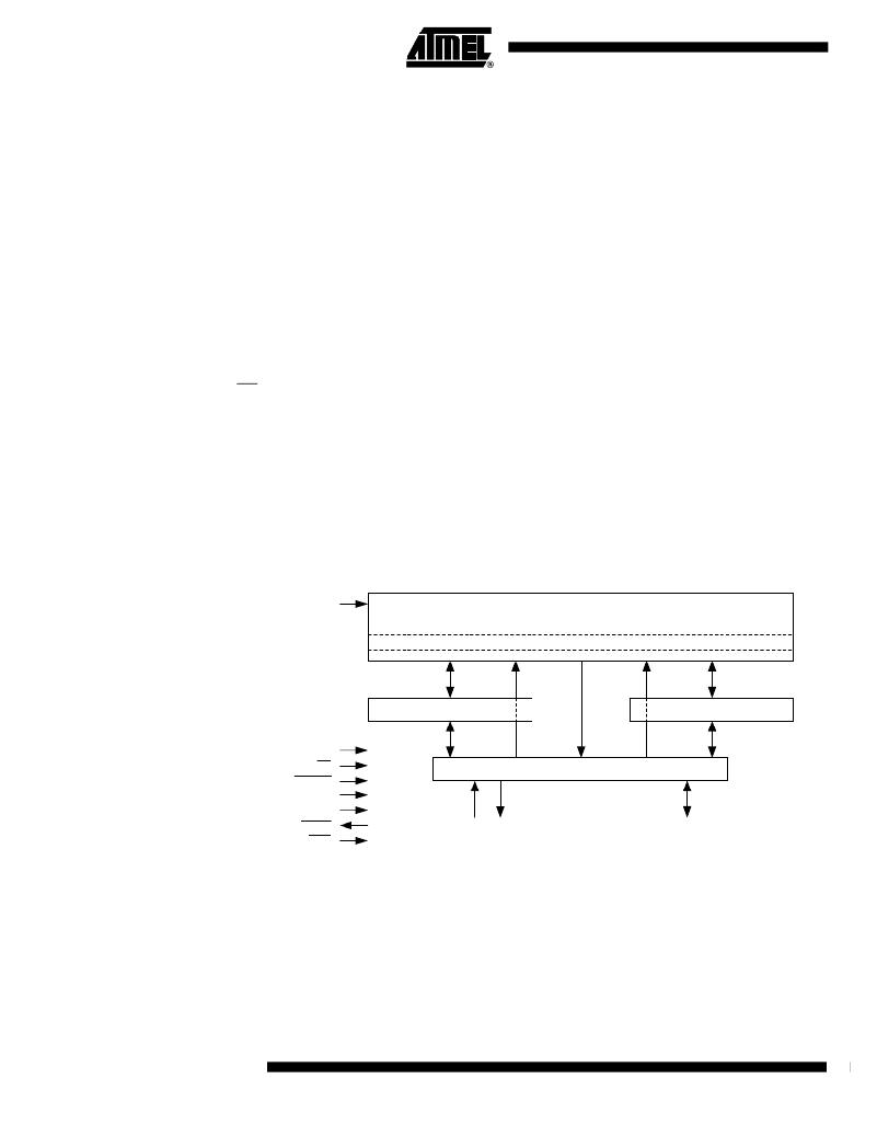
�Block� Diagram�
�WP�
�PAGE� (1056� BYTES)�
�FLASH� MEMORY� ARRAY�
�SCK/CLK�
�CS�
�RESET�
�VCC�
�GND�
�BUFFER� 1� (1056� BYTES)�
�I/O� INTERFACE�
�BUFFER� 2� (1056� BYTES)�
�RDY/BUSY�
�SI�
�SO�
�I/O7� -� I/O0�
�SER/PAR�
�Memory� Array�
�To� provide� optimal� flexibility,� the� memory� array� of� the� AT45DB642� is� divided� into� three� levels�
�of� granularity� comprising� of� sectors,� blocks� and� pages.� The� “� Memory� Architecture� Diagram� ”�
�illustrates� the� breakdown� of� each� level� and� details� the� number� of� pages� per� sector� and� block.�
�All� program� operations� to� the� DataFlash� occur� on� a� page-by-page� basis;� however,� the� optional�
�erase� operations� can� be� performed� at� the� block� or� page� level.�
�2�
�AT45DB642�
�1638F� –� DFLSH� –� 09/02�
�相关PDF资料 |
PDF描述 |
|---|---|
| T95V225K025HSAL | CAP TANT 2.2UF 25V 10% 1410 |
| EBC17DCAD | CONN EDGECARD 34POS R/A .100 SLD |
| CDBD2045-G | DIODE SCHOTTKY 45V 20A D2PAK |
| RKZ-0505S/P | CONV DC/DC 2W 05VIN 05VOUT |
| CDBD2040-HF | DIODE SCHOTTKY 40V 20A D2PAK |
相关代理商/技术参数 |
参数描述 |
|---|---|
| AT45DB64D2-CNU | 制造商:ATMEL 制造商全称:ATMEL Corporation 功能描述:32-bit Microcontrollers |
| AT45DCB002 | 功能描述:存储卡 2M bit RoHS:否 制造商:Olimex Ltd. 产品:SD 存储容量: 连续读取: 连续写入: 有源模式电流: 工作电源电压: 最大工作温度: 尺寸: |
| AT45DCB002D | 功能描述:存储卡 CARD 2M BYTE RoHS:否 制造商:Olimex Ltd. 产品:SD 存储容量: 连续读取: 连续写入: 有源模式电流: 工作电源电压: 最大工作温度: 尺寸: |
| AT45DCB004 | 功能描述:DATAFLASH CARD 4MEGABYTE RoHS:否 类别:存储卡,模块 >> 存储器,PC 卡 系列:- 标准包装:30 系列:- 存储容量:8GB 存储器类型:存储卡 - Extreme III SD? |
| AT45DCB004C | 制造商:ATMEL 制造商全称:ATMEL Corporation 功能描述:4-megabyte 2.7-volt DataFlash Card |
发布紧急采购,3分钟左右您将得到回复。