- 您现在的位置:买卖IC网 > PDF目录381463 > AT49BV8192A-20CC (ATMEL CORP) 8-Megabit 1M x 8/ 512K x 16 CMOS Flash Memory PDF资料下载
参数资料
| 型号: | AT49BV8192A-20CC |
| 厂商: | ATMEL CORP |
| 元件分类: | DRAM |
| 英文描述: | 8-Megabit 1M x 8/ 512K x 16 CMOS Flash Memory |
| 中文描述: | 1M X 8 FLASH 5V PROM, 200 ns, PBGA48 |
| 封装: | CBGA-48 |
| 文件页数: | 2/16页 |
| 文件大小: | 246K |
| 代理商: | AT49BV8192A-20CC |
AT49BV008A(T)/8192A(T)
2
The device is erased by executing the erase command
sequence; the device internally controls the erase opera-
tion. The memory is divided into four blocks for erase oper-
ations. There are two 4K word parameter block sections,
the boot block, and the main memory array block. The typi-
cal number of program and erase cycles is in excess of
10,000 cycles.
The optional 8K word boot block section includes a repro-
gramming lock out feature to provide data integrity. This
feature is enabled by a command sequence. Once the boot
block programming lockout feature is enabled, the data in
the boot block cannot be changed when input levels of 3.6
volts or less are used. The boot sector is designed to con-
tain user secure code.
For the AT49BV8192A(T), the BYTE pin controls whether
the device data I/O pins operate in the byte or word config-
uration. If the BYTE pin is set at a logic “1” or left open, the
device is in word configuration, I/O0 - I/O15 are active and
controlled by CE and OE.
If the BYTE pin is set at logic “0”, the device is in byte con-
figuration, and only data I/O pins I/O0 - I/O7 are active and
controlled by CE and OE. The data I/O pins I/O8 - I/O14
are tri-stated and the I/O15 pin is used as an input for the
LSB (A-1) address function.
An optional V
PP
pin is available to improve program/erase
times. Please contact Atmel for more information.
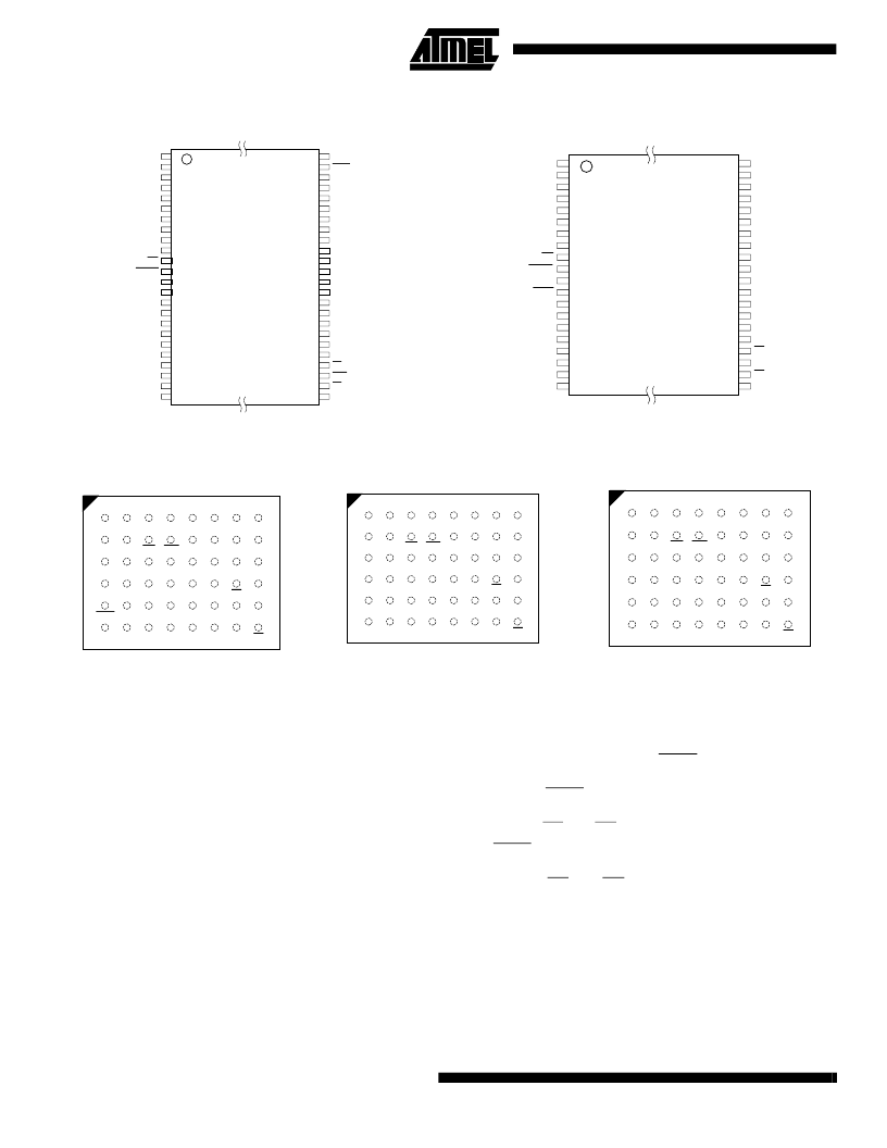
AT49BV8192A(T) TSOP Top View
Type 1
1
2
3
4
5
6
7
8
9
10
11
12
13
14
15
16
17
18
19
20
21
22
23
24
48
47
46
45
44
43
42
41
40
39
38
37
36
35
34
33
32
31
30
29
28
27
26
25
A15
A14
A13
A12
A11
A10
A9
A8
NC
NC
WE
RESET
*NC/VPP
NC
NC
A18
A17
A7
A6
A5
A4
A3
A2
A1
A16
BYTE
GND
I/O15 / A-1
I/O7
I/O14
I/O6
I/O13
I/O5
I/O12
I/O4
VCC
I/O11
I/O3
I/O10
I/O2
I/O9
I/O1
I/O8
I/O0
OE
GND
CE
A0
AT49BV008A(T) TSOP Top View
Type 1
1
2
3
4
5
6
7
8
9
10
11
12
13
14
15
16
17
18
19
20
40
39
38
37
36
35
34
33
32
31
30
29
28
27
26
25
24
23
22
21
A16
A15
A14
A13
A12
A11
A9
A8
WE
RESET
*NC/VPP
RDY/BUSY
A18
A7
A6
A5
A4
A3
A2
A1
A17
GND
NC
A-1
A10
I/O7
I/O6
I/O5
I/O4
VCC
VCC
NC
I/O3
I/O2
I/O1
I/O0
OE
GND
CE
A0
AT49BV8192A(T)
CBGA Top View (Ball Down)
A
B
C
D
E
F
1
2
3
4
5
6
7
A13
A14
A15
A16
BYTE
GND
A11
A10
A12
I/O14
I/O15
I/O7
A8
WE
A9
I/O5
I/O6
I/O13
*NC/VPP
RST
NC
I/O11
I/O12
I/O4
NC
A18
NC
I/O2
I/O3
VCC
NC
A17
A6
I/O8
I/O9
I/O10
A7
A5
A3
CE
I/O0
I/O1
8
A4
A2
A1
A0
GND
OE
AT49BV008A(T) Standard Pin Definition
CBGA Top View (Ball Down)
A
B
C
D
E
F
1
2
3
4
5
6
7
A13
A14
A15
A16
NC
GND
A11
A10
A12
NC
A-1
I/O7
A8
WE
A9
I/O5
I/O6
NC
VPP
RST
NC
NC
NC
I/O4
NC
A18
NC
I/O2
I/O3
VCC
NC
A17
A6
NC
NC
NC
A7
A5
A3
CE
I/O0
I/O1
8
A4
A2
A1
A0
GND
OE
AT49BV008A(T) Alternate Pin Definition
CBGA Top View (Ball Down)
A
B
C
D
E
F
1
2
3
4
5
6
7
A14
A15
A16
A17
NC
GND
A12
A10
A13
NC
A11
I/O7
A8
WE
A9
I/O5
I/O6
NC
VPP
RST
NC
NC
NC
I/O4
NC
A19
NC
I/O2
I/O3
VCC
NC
A18
A6
NC
NC
NC
A7
A5
A3
CE
I/O0
I/O1
8
A4
A2
A1
A0
GND
OE
*Standard device is a NC. Please contact Atmel for VPP option.
相关PDF资料 |
PDF描述 |
|---|---|
| AT49BV8192A-20CI | 8-Megabit 1M x 8/ 512K x 16 CMOS Flash Memory |
| AT49BV8192A-20TC | 8-Megabit 1M x 8/ 512K x 16 CMOS Flash Memory |
| AT49BV8192A-20TI | 8-Megabit 1M x 8/ 512K x 16 CMOS Flash Memory |
| AT49BV8192A | 8-Megabit 1M x 8/ 512K x 16 CMOS Flash Memory |
| AT49BV8192AT | 8-Megabit 1M x 8/ 512K x 16 CMOS Flash Memory |
相关代理商/技术参数 |
参数描述 |
|---|---|
| AT49BV8192A-20CI | 制造商:ATMEL 制造商全称:ATMEL Corporation 功能描述:8-Megabit 1M x 8/ 512K x 16 CMOS Flash Memory |
| AT49BV8192A-20RC | 制造商:未知厂家 制造商全称:未知厂家 功能描述:x8/x16 Flash EEPROM |
| AT49BV8192A-20RI | 制造商:未知厂家 制造商全称:未知厂家 功能描述:x8/x16 Flash EEPROM |
| AT49BV8192A-20TC | 制造商:ATMEL 制造商全称:ATMEL Corporation 功能描述:8-Megabit 1M x 8/ 512K x 16 CMOS Flash Memory |
| AT49BV8192A-20TI | 制造商:ATMEL 制造商全称:ATMEL Corporation 功能描述:8-Megabit 1M x 8/ 512K x 16 CMOS Flash Memory |
发布紧急采购,3分钟左右您将得到回复。