- 您现在的位置:买卖IC网 > PDF目录381473 > AT49F040T-90PC (ATMEL CORP) 4-Megabit 512K x 8 5-volt Only CMOS Flash Memory PDF资料下载
参数资料
| 型号: | AT49F040T-90PC |
| 厂商: | ATMEL CORP |
| 元件分类: | DRAM |
| 英文描述: | 4-Megabit 512K x 8 5-volt Only CMOS Flash Memory |
| 中文描述: | 512K X 8 FLASH 5V PROM, 90 ns, PDIP32 |
| 封装: | 0.600 INCH, PLASTIC, DIP-32 |
| 文件页数: | 2/12页 |
| 文件大小: | 229K |
| 代理商: | AT49F040T-90PC |
AT49F040/040T
2
To allow for simple in-system reprogrammability, the
AT49F040 does not require high input voltages for pro-
gramming. Five-volt-only commands determine the read
and programming operation of the device. Reading data
out of the device is similar to reading from an EPROM.
Reprogramming the AT49F040 is performed by erasing
the entire 4 megabits of memory and then programming on
a byte by byte basis. The byte programming time is a fast
50
μ
s. The end of a program cycle can be optionally
detected by the DATA polling feature. Once the end of a
byte program cycle has been detected, a new access for a
read or program can begin. The typical number of program
and erase cycles is in excess of 10,000 cycles.
The optional 16K bytes boot block section includes a repro-
gramming write lock out feature to provide data integrity.
The boot sector is designed to contain user secure code,
and when the feature is enabled, the boot sector is perma-
nently protected from being reprogrammed.
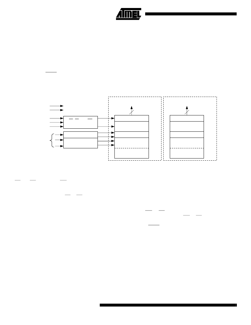
Block Diagram
Device Operation
READ:
The AT49F040 is accessed like an EPROM. When
CE and OE are low and WE is high, the data stored at the
memory location determined by the address pins is
asserted on the outputs. The outputs are put in the high
impedance state whenever CE or OE is high. This dual-line
control gives designers flexibility in preventing bus conten-
tion.
ERASURE:
Before a byte can be reprogrammed, the
512K bytes memory array (or 496K bytes if the boot block
featured is used) must be erased. The erased state of the
memory bits is a logical “1”. The entire device can be
erased at one time by using a 6-byte software code. The
software chip erase code consists of 6-byte load com-
mands to specific address locations with a specific data
pattern (please refer to the Chip Erase Cycle Waveforms).
After the software chip erase has been initiated, the device
will internally time the erase operation so that no external
clocks are required. The maximum time needed to erase
the whole chip is t
EC
. If the boot block lockout feature has
been enabled, the data in the boot sector will not be
erased.
BYTE PROGRAMMING:
Once the memory array is erased,
the device is programmed (to a logical “0”) on a byte-by-
byte basis. Please note that a data ”0" cannot be pro-
grammed back to a “1”; only erase operations can convert
“0”s to “1”s. Programming is accomplished via the internal
device command register and is a 4 bus cycle operation
(please refer to the Command Definitions table). The
device will automatically generate the required internal pro-
gram pulses.
The program cycle has addresses latched on the falling
edge of WE or CE, whichever occurs last, and the data
latched on the rising edge of WE or CE, whichever occurs
first. Programming is completed after the specified t
BP
cycle
time. The DATA polling feature may also be used to indi-
cate the end of a program cycle.
BOOT BLOCK PROGRAMMING LOCKOUT:
The device
has one designated block that has a programming lockout
feature. This feature prevents programming of data in the
designated block once the feature has been enabled. The
size of the block is 16K bytes. This block, referred to as the
boot block, can contain secure code that is used to bring up
the system. Enabling the lockout feature will allow the boot
code to stay in the device while data in the rest of the
device is updated. This feature does not have to be acti-
vated; the boot block's usage as a write protected region is
optional to the user. The address range of the AT49F040
OE, CE, AND WE
LOGIC
Y DECODER
X DECODER
INPUT/OUTPUT
BUFFERS
DATA LATCH
Y-GATING
OPTIONAL BOOT
BLOCK (16K BYTES)
MAIN MEMORY
(496K BYTES)
OE
WE
CE
ADDRESS
INPUTS
V
CC
GND
DATA INPUTS/OUTPUTS
I/O7 - I/O0
8
03FFFH
00000H
INPUT/OUTPUT
BUFFERS
DATA LATCH
Y-GATING
OPTIONAL BOOT
BLOCK (16K BYTES)
MAIN MEMORY
(496K BYTES)
7C000H
00000H
AT49F040T
AT49F040
DATA INPUTS/OUTPUTS
I/O7 - I/O0
8
7FFFFH
7FFFFH
相关PDF资料 |
PDF描述 |
|---|---|
| AT49F040T-90PI | 4-Megabit 512K x 8 5-volt Only CMOS Flash Memory |
| AT49F040T-90TC | 4-Megabit 512K x 8 5-volt Only CMOS Flash Memory |
| AT49F040T-90TI | 4-Megabit 512K x 8 5-volt Only CMOS Flash Memory |
| AT49F040 | 4 Megabit 512K x 8 5-volt Only CMOS Flash Memory |
| AT49F040-12TC | 4-Megabit 512K x 8 5-volt Only CMOS Flash Memory |
相关代理商/技术参数 |
参数描述 |
|---|---|
| AT49F040T-90PI | 制造商:ATMEL 制造商全称:ATMEL Corporation 功能描述:4-Megabit 512K x 8 5-volt Only CMOS Flash Memory |
| AT49F040T-90TC | 制造商:ATMEL 制造商全称:ATMEL Corporation 功能描述:4-Megabit 512K x 8 5-volt Only CMOS Flash Memory |
| AT49F040T-90TI | 制造商:ATMEL 制造商全称:ATMEL Corporation 功能描述:4-Megabit 512K x 8 5-volt Only CMOS Flash Memory |
| AT49F080 | 制造商:ATMEL 制造商全称:ATMEL Corporation 功能描述:8-Megabit 1M x 8 5-volt Only Flash Memory |
| AT49F080-12CC | 制造商:ATMEL 制造商全称:ATMEL Corporation 功能描述:8-Megabit 1M x 8 5-volt Only Flash Memory |
发布紧急采购,3分钟左右您将得到回复。