- 您现在的位置:买卖IC网 > PDF目录381457 > AT49LV002N-12TI (ATMEL CORP) LM4884 Boomer ® Audio Power Amplifier Series 2.1W Differential Input, BTL Output Stereo Audio Amplifier with RF Suppression and Shutdown; Package: TSSOP EXP PAD; No of Pins: 20 PDF资料下载
参数资料
| 型号: | AT49LV002N-12TI |
| 厂商: | ATMEL CORP |
| 元件分类: | DRAM |
| 英文描述: | LM4884 Boomer ® Audio Power Amplifier Series 2.1W Differential Input, BTL Output Stereo Audio Amplifier with RF Suppression and Shutdown; Package: TSSOP EXP PAD; No of Pins: 20 |
| 中文描述: | 256K X 8 FLASH 3V PROM, 120 ns, PDSO32 |
| 封装: | 8 X 20 MM, PLASTIC, TSOP1-32 |
| 文件页数: | 2/20页 |
| 文件大小: | 171K |
| 代理商: | AT49LV002N-12TI |
AT49BV/LV002(N)(T)
2
AT49BV/LV002N(T) pin 1 for the DIP and PLCC packages
and pin 9 for the TSOP package are don’t connect pins.
To allow for simple in-system reprogrammability, the
AT49BV/LV002(N)(T) does not require high input voltages
for programming. Five-volt-only commands determine the
read and programming operation of the device. Reading
data out of the device is similar to reading from an EPROM;
it has standard CE, OE, and WE inputs to avoid bus con-
tention. Reprogramming the AT49BV/LV002(N)(T) is per-
formed by erasing a block of data and then programming
on a byte by byte basis. The byte programming time is a
fast 50
μ
s. The end of a program cycle can be optionally
detected by the DATA polling feature. Once the end of a
byte program cycle has been detected, a new access for a
read or program can begin. The typical number of program
and erase cycles is in excess of 10,000 cycles.
The device is erased by executing the erase command
sequence; the device internally controls the erase opera-
tions. There are two 8K byte parameter block sections and
two main memory blocks.
The device has the capability to protect the data in the boot
block; this feature is enabled by a command sequence.
The 16K-byte boot block section includes a reprogramming
lock out feature to provide data integrity. The boot sector is
designed to contain user secure code, and when the fea-
ture is enabled, the boot sector is protected from being
reprogrammed.
In the AT49BV/LV002N(T), once the boot block program-
ming lockout feature is enabled, the contents of the boot
block are permanent and cannot be changed. In the
AT49BV/LV002(T), once the boot block programming lock-
out feature is enabled, the contents of the boot block can-
not be changed with input voltage levels of 5.5 volts or less.
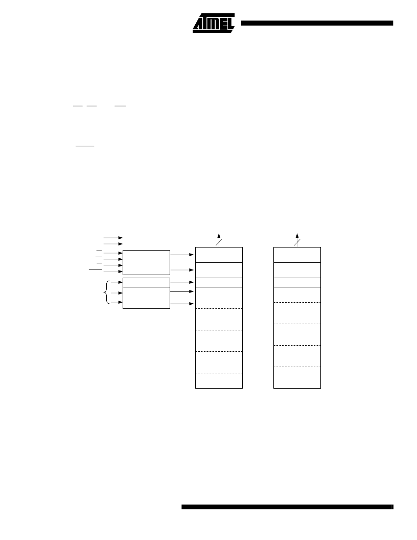
Block Diagram
CONTROL
LOGIC
Y DECODER
PARAMETER
BLOCK 1
(8K BYTES)
BOOT BLOCK
(16K BYTES)
OE
WE
CE
RESET
ADDRESS
INPUTS
V
CC
GND
AT49BV/LV002(N)
DATA INPUTS/OUTPUTS
I/O7 - I/O0
8
X DECODER
PARAMETER
BLOCK 2
(8K BYTES)
MAIN MEMORY
BLOCK 1
(96K BYTES)
MAIN MEMORY
BLOCK 2
(128K BYTES)
PROGRAM
DATA LATCHES
Y-GATING
INPUT/OUTPUT
BUFFERS
3FFFF
20000
1FFFF
08000
07FFF
06000
05FFF
04000
03FFF
00000
PARAMETER
BLOCK 1
(8K BYTES)
BOOT BLOCK
(16K BYTES)
AT49BV/LV002(N)T
DATA INPUTS/OUTPUTS
I/O7 - I/O0
8
PARAMETER
BLOCK 2
(8K BYTES)
MAIN MEMORY
BLOCK 1
(96K BYTES)
MAIN MEMORY
BLOCK 2
(128K BYTES)
PROGRAM
DATA LATCHES
Y-GATING
INPUT/OUTPUT
BUFFERS
3FFFF
3C000
3BFFF
3A000
39FFF
38000
37FFF
20000
1FFFF
00000
相关PDF资料 |
PDF描述 |
|---|---|
| AT49LV002N-12VC | 2-Megabit 256K x 8 Single 2.7-Volt Battery-Voltage Flash Memory |
| AT49LV002N-12VI | LM48860 Ground-Referenced, Ultra Low Noise, Fixed Gain Stereo Headphone Amplifier; Package: MICRO SMD; No of Pins: 12 |
| AT49LV002N-70JC | LM48860 Ground-Referenced, Ultra Low Noise, Fixed Gain Stereo Headphone Amplifier |
| AT49LV002N-70JI | LM48860 Ground-Referenced, Ultra Low Noise, Fixed Gain Stereo Headphone Amplifier; Package: MICRO SMD; No of Pins: 12 |
| AT49LV002N-70PC | LM48861 PowerWise® Ground-Referenced, Ultra Low Noise, Stereo Headphone Amplifier; Package: MICRO SMD; No of Pins: 12 |
相关代理商/技术参数 |
参数描述 |
|---|---|
| AT49LV002N-12VC | 功能描述:闪存 256K x 8 (2M bit) RoHS:否 制造商:ON Semiconductor 数据总线宽度:1 bit 存储类型:Flash 存储容量:2 MB 结构:256 K x 8 定时类型: 接口类型:SPI 访问时间: 电源电压-最大:3.6 V 电源电压-最小:2.3 V 最大工作电流:15 mA 工作温度:- 40 C to + 85 C 安装风格:SMD/SMT 封装 / 箱体: 封装:Reel |
| AT49LV002N-12VI | 功能描述:IC FLASH 2MBIT 120NS 32VSOP RoHS:否 类别:集成电路 (IC) >> 存储器 系列:- 标准包装:378 系列:- 格式 - 存储器:闪存 存储器类型:FLASH 存储容量:8M(1M x 8,512K x 16) 速度:110ns 接口:并联 电源电压:2.7 V ~ 3.6 V 工作温度:-40°C ~ 85°C 封装/外壳:48-CBGA 供应商设备封装:48-CBGA(7x7) 包装:托盘 |
| AT49LV002N-70VI | 功能描述:IC FLASH 2MBIT 70NS 32VSOP RoHS:否 类别:集成电路 (IC) >> 存储器 系列:- 标准包装:96 系列:- 格式 - 存储器:闪存 存储器类型:FLASH 存储容量:16M(2M x 8,1M x 16) 速度:70ns 接口:并联 电源电压:2.65 V ~ 3.6 V 工作温度:-40°C ~ 85°C 封装/外壳:48-TFSOP(0.724",18.40mm 宽) 供应商设备封装:48-TSOP 包装:托盘 |
| AT49LV002N-90JC | 功能描述:闪存 256K x 8 (2M bit) RoHS:否 制造商:ON Semiconductor 数据总线宽度:1 bit 存储类型:Flash 存储容量:2 MB 结构:256 K x 8 定时类型: 接口类型:SPI 访问时间: 电源电压-最大:3.6 V 电源电压-最小:2.3 V 最大工作电流:15 mA 工作温度:- 40 C to + 85 C 安装风格:SMD/SMT 封装 / 箱体: 封装:Reel |
| AT49LV002N-90JI | 功能描述:IC FLASH 2MBIT 90NS 32PLCC RoHS:否 类别:集成电路 (IC) >> 存储器 系列:- 标准包装:378 系列:- 格式 - 存储器:闪存 存储器类型:FLASH 存储容量:8M(1M x 8,512K x 16) 速度:110ns 接口:并联 电源电压:2.7 V ~ 3.6 V 工作温度:-40°C ~ 85°C 封装/外壳:48-CBGA 供应商设备封装:48-CBGA(7x7) 包装:托盘 |
发布紧急采购,3分钟左右您将得到回复。