- 您现在的位置:买卖IC网 > PDF目录362501 > AT77C101B-CB02C Signal Conditioner PDF资料下载
参数资料
| 型号: | AT77C101B-CB02C |
| 英文描述: | Signal Conditioner |
| 中文描述: | 信号调理 |
| 文件页数: | 14/23页 |
| 文件大小: | 415K |
| 代理商: | AT77C101B-CB02C |
14
AT77C101B
2150A
–
BIOM
–
02/02
Analog-to-Digital
Converter/
Reconstructing an 8-bit
Fingerprint Image
An Analog-to-Digital Converter (ADC) is used to convert the analog signal coming from
the pixel into digital data that can be used by a processor.
As the data rate for parallel port and USB is in the range of 1 MB per second, and at
least a rate of 500 frames per second is needed to reconstruct the image with a fair
sweeping speed for the finger, two 4-bit ADCs have been used to output 2 pixels at a
time on 1 byte.
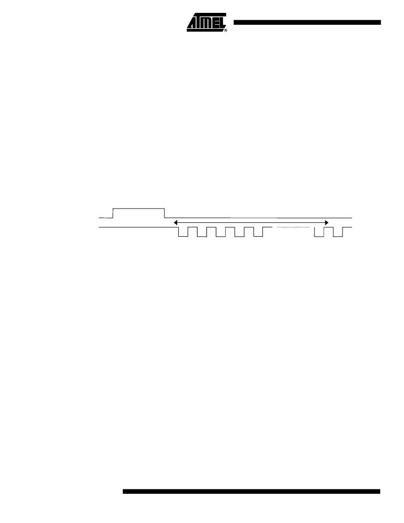
Start Sequence
A reset is not necessary between each frame acquisition.
Start sequence must consist of:
1.
Set the RST pin to high
2.
Set the RST pin to low
3.
Send 4 clock pulses (due to pipe-line)
4.
Send clock pulses to skip the first frame
Note that the first frame never contains relevant information because the integration
time is not correct.
Figure 10.
Start Sequence
Reading the Frames
A frame consists of 280 true columns + 1 dummy column of 8 pixels. As two pixels are
output at a time, a system must send 281x4 = 1124 clock pulses to read one frame.
Reset must be low when reading the frames.
Read One Byte/Output
Enable
Clock is taken into account on the falling edge and data are output on the rising edge.
For each clock pulse, after the start sequence, a new byte is output on the Do0-3, De0-
3 pins. This byte contains 2 pixels: 4-bit on Do0-3 (odd pixels), 4-bit on De0-3 (even
pixels).
To output the data, the output enable (OE) pin must be low. When OE is high, the Do0-
3 and De0-3 pins are in high-impedance state. This facilitates an easy connection to a
microprocessor bus without additional circuitry since data output can be enabled using a
chip select signal. Note that the AT77C101B is always sending data: there is no data
exchange to perform using read/write mode.
Power Supply Noise
IMPORTANT: When a falling edge is applied on OE (i.e when the Output Enable
becomes active), then some current is drained from the power supply to drive the 8 out-
puts, producing some noise. It is important to avoid such noise just after the falling edge
of the clock PCLK, when the pixels information is evaluated: the timing diagram figure 5
and time T
NOOE
defines the interval time where the power supply must be as quiet as
possible.
1
4
3
1
2
1
1124
Clock PCLK
Reset RST
4+1124 clock pulses to skip the first frame
相关PDF资料 |
PDF描述 |
|---|---|
| AT77C101B-CB01C | Signal Conditioner |
| AT78C1501 | AT78C1501 [Updated 7/02. 15 Pages] DVD Interface Controller supporting all current DVD and CD writeable and rewriteable standards. |
| AT78C1501-208TC | Controller Miscellaneous - Datasheet Reference |
| AT78C1504 | Controller Miscellaneous - Datasheet Reference |
| AT80C51ID2 | AT83C51RB2. AT83C51RC2. AT83C51IC2. AT80C51ID2 Errata [Updated 7/03. 4 Pages] |
相关代理商/技术参数 |
参数描述 |
|---|---|
| AT77C102B | 制造商:ATMEL 制造商全称:ATMEL Corporation 功能描述:Thermal Fingerprint Sensor with 0.4 mm x 14 mm (0.02 x 0.55) Sensing Area and Digital Output (On-chip ADC) |
| AT77C102B_07 | 制造商:ATMEL 制造商全称:ATMEL Corporation 功能描述:Thermal Fingerprint Sensor with 0.4 mm x 14 mm (0.02" x 0.55") Sensing Area and Digital Output (On-chip ADC) |
| AT77C102B-CB01YV | 制造商:ATMEL 制造商全称:ATMEL Corporation 功能描述:Thermal Fingerprint Sensor with 0.4 mm x 14 mm (0.02" x 0.55") Sensing Area and Digital Output (On-chip ADC) |
| AT77C102B-CB01YV- | 制造商:ATMEL 制造商全称:ATMEL Corporation 功能描述:Thermal Fingerprint Sensor with 0.4 mm x 14 mm (0.02 x 0.55) Sensing Area and Digital Output (On-chip ADC) |
| AT77C102B-CB02YV | 制造商:ATMEL 制造商全称:ATMEL Corporation 功能描述:Thermal Fingerprint Sensor with 0.4 mm x 14 mm (0.02" x 0.55") Sensing Area and Digital Output (On-chip ADC) |
发布紧急采购,3分钟左右您将得到回复。