参数资料
| 型号: | AT87251G2D-RLTUM |
| 厂商: | Atmel |
| 文件页数: | 77/77页 |
| 文件大小: | 0K |
| 描述: | IC MCU 8/16BIT 32K OTP 44-VQFP |
| 标准包装: | 160 |
| 系列: | 8x251 |
| 核心处理器: | C251 |
| 芯体尺寸: | 8/16-位 |
| 速度: | 24MHz |
| 连通性: | EBI/EMI,I²C,Microwire,SPI,UART/USART |
| 外围设备: | POR,PWM,WDT |
| 输入/输出数: | 32 |
| 程序存储器容量: | 32KB(32K x 8) |
| 程序存储器类型: | OTP |
| RAM 容量: | 1K x 8 |
| 电压 - 电源 (Vcc/Vdd): | 4.5 V ~ 5.5 V |
| 振荡器型: | 内部 |
| 工作温度: | -40°C ~ 85°C |
| 封装/外壳: | 44-LQFP |
| 包装: | 托盘 |
第1页第2页第3页第4页第5页第6页第7页第8页第9页第10页第11页第12页第13页第14页第15页第16页第17页第18页第19页第20页第21页第22页第23页第24页第25页第26页第27页第28页第29页第30页第31页第32页第33页第34页第35页第36页第37页第38页第39页第40页第41页第42页第43页第44页第45页第46页第47页第48页第49页第50页第51页第52页第53页第54页第55页第56页第57页第58页第59页第60页第61页第62页第63页第64页第65页第66页第67页第68页第69页第70页第71页第72页第73页第74页第75页第76页当前第77页
9
AT/TSC8x251G2D
4135F–8051–11/06
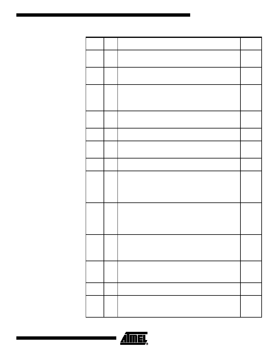
T1:0
I/O
Timer 1:0 External Clock Inputs
When timer 1:0 operates as a counter, a falling edge on the T1:0 pin
increments the count.
–
T2
I/O
Timer 2 Clock Input/Output
For the timer 2 capture mode, T2 is the external clock input. For the Timer 2
clock-out mode, T2 is the clock output.
P1.0
T2EX
I
Timer 2 External Input
In timer 2 capture mode, a falling edge initiates a capture of the timer 2
registers. In auto-reload mode, a falling edge causes the timer 2 register to
be reloaded. In the up-down counter mode, this signal determines the
count direction: 1 = up, 0 = down.
P1.1
TXD
O
Transmit Serial Data
TXD outputs the shift clock in serial I/O mode 0 and transmits data in serial
I/O modes 1, 2 and 3.
P3.1
VDD
PWR
Digital Supply Voltage
Connect this pin to +5V or +3V supply voltage.
–
VPP
I
Programming Supply Voltage
The programming supply voltage is applied to this input for programming
the on-chip EPROM/OTPROM.
–
VSS
GND
Circuit Ground
Connect this pin to ground.
–
VSS1
GND
Secondary Ground 1
This ground is provided to reduce ground bounce and improve power
supply bypassing. Connection of this pin to ground is recommended.
However, when using the TSC80251G2D as a pin-for-pin replacement for a
8xC51 product, VSS1 can be unconnected without loss of compatibility.
Not available on DIP package.
–
VSS2
GND
Secondary Ground 2
This ground is provided to reduce ground bounce and improve power
supply bypassing. Connection of this pin to ground is recommended.
However, when using the TSC80251G2D as a pin-for-pin replacement for a
8xC51 product, VSS2 can be unconnected without loss of compatibility.
Not available on DIP package.
–
WAIT#
I
Real-time Synchronous Wait States Input
The real-time WAIT# input is enabled by setting RTWE bit in WCON
(S:A7h). During bus cycles, the external memory system can signal
‘system ready’ to the microcontroller in real time by controlling the WAIT#
input signal.
P1.6
WCLK
O
Wait Clock Output
The real-time WCLK output is enabled by setting RTWCE bit in WCON
(S:A7h). When enabled, the WCLK output produces a square wave signal
with a period of one half the oscillator frequency.
P1.7
WR#
O
Write
Write signal output to external memory.
P3.6
XTAL1
I
Input to the on-chip inverting oscillator amplifier
To use the internal oscillator, a crystal/resonator circuit is connected to this
pin. If an external oscillator is used, its output is connected to this pin.
XTAL1 is the clock source for internal timing.
–
Table 2.
Product Name Signal Description (Continued)
Signal
Name
Type
Description
Alternate
Function
相关PDF资料 |
PDF描述 |
|---|---|
| AT87C51RB2-SLRUM | MCU ROMLESS 16K OTP 44-PLCC |
| AT87C52X2-RLRUM | MCU ROMLESS 32X2 3V 44-VQFP |
| AT87C58X2-SLRUM | MCU 8051 32K EPROM 44PLCC |
| AT87F51-24PI | IC MICRO CTRL 24MHZ 40DIP |
| AT87F52-24PC | IC MICRO CTRL 24MHZ 40DIP |
相关代理商/技术参数 |
参数描述 |
|---|---|
| AT87251G2D-SLSUL | 功能描述:8位微控制器 -MCU Microcontroller RoHS:否 制造商:Silicon Labs 核心:8051 处理器系列:C8051F39x 数据总线宽度:8 bit 最大时钟频率:50 MHz 程序存储器大小:16 KB 数据 RAM 大小:1 KB 片上 ADC:Yes 工作电源电压:1.8 V to 3.6 V 工作温度范围:- 40 C to + 105 C 封装 / 箱体:QFN-20 安装风格:SMD/SMT |
| AT87251G2D-SLSUM | 功能描述:8位微控制器 -MCU OTP 8/16bit St 5V 24MHz RoHS:否 制造商:Silicon Labs 核心:8051 处理器系列:C8051F39x 数据总线宽度:8 bit 最大时钟频率:50 MHz 程序存储器大小:16 KB 数据 RAM 大小:1 KB 片上 ADC:Yes 工作电源电压:1.8 V to 3.6 V 工作温度范围:- 40 C to + 105 C 封装 / 箱体:QFN-20 安装风格:SMD/SMT |
| AT875 | 制造商:POSEICO 制造商全称:POSEICO 功能描述:PHASE CONTROL THYRISTOR |
| AT875LT | 制造商:POSEICO 制造商全称:POSEICO 功能描述:PHASE CONTROL THYRISTOR |
| AT875LTS44 | 制造商:POSEICO 制造商全称:POSEICO 功能描述:PHASE CONTROL THYRISTOR |
发布紧急采购,3分钟左右您将得到回复。