参数资料
| 型号: | AT89C5132-ROTUL |
| 厂商: | Atmel |
| 文件页数: | 37/182页 |
| 文件大小: | 0K |
| 描述: | IC 8051 MCU FLASH 64K USB 80TQFP |
| 产品培训模块: | MCU Product Line Introduction |
| 标准包装: | 450 |
| 系列: | AT89C513x |
| 核心处理器: | C52X2 |
| 芯体尺寸: | 8-位 |
| 速度: | 20MHz |
| 连通性: | IDE/ATAPI,I²C,MMC,PCM,SPI,UART/USART,USB |
| 外围设备: | I²S,POR,WDT |
| 输入/输出数: | 44 |
| 程序存储器容量: | 64KB(64K x 8) |
| 程序存储器类型: | 闪存 |
| EEPROM 大小: | 4K x 8 |
| RAM 容量: | 2.25K x 8 |
| 电压 - 电源 (Vcc/Vdd): | 2.7 V ~ 3.3 V |
| 数据转换器: | A/D 2x10b |
| 振荡器型: | 内部 |
| 工作温度: | -40°C ~ 85°C |
| 封装/外壳: | 80-LQFP |
| 包装: | 托盘 |
| 配用: | AT89OCD-01-ND - USB EMULATOR FOR AT8XC51 MCU |
第1页第2页第3页第4页第5页第6页第7页第8页第9页第10页第11页第12页第13页第14页第15页第16页第17页第18页第19页第20页第21页第22页第23页第24页第25页第26页第27页第28页第29页第30页第31页第32页第33页第34页第35页第36页当前第37页第38页第39页第40页第41页第42页第43页第44页第45页第46页第47页第48页第49页第50页第51页第52页第53页第54页第55页第56页第57页第58页第59页第60页第61页第62页第63页第64页第65页第66页第67页第68页第69页第70页第71页第72页第73页第74页第75页第76页第77页第78页第79页第80页第81页第82页第83页第84页第85页第86页第87页第88页第89页第90页第91页第92页第93页第94页第95页第96页第97页第98页第99页第100页第101页第102页第103页第104页第105页第106页第107页第108页第109页第110页第111页第112页第113页第114页第115页第116页第117页第118页第119页第120页第121页第122页第123页第124页第125页第126页第127页第128页第129页第130页第131页第132页第133页第134页第135页第136页第137页第138页第139页第140页第141页第142页第143页第144页第145页第146页第147页第148页第149页第150页第151页第152页第153页第154页第155页第156页第157页第158页第159页第160页第161页第162页第163页第164页第165页第166页第167页第168页第169页第170页第171页第172页第173页第174页第175页第176页第177页第178页第179页第180页第181页第182页
131
4173E–USB–09/07
AT89C5132
20. Two-wire Interface (TWI) Controller
The AT89C5132 implements a TWI controller supporting the four standard master and slave
modes with multimaster capability. Thus, it allows connection of slave devices like LCD control-
ler, audio DAC, etc., but also external master controlling where the AT89C5132 is used as a
peripheral of a host.
The TWI bus is a bi-directional TWI serial communication standard. It is designed primarily for
simple but efficient integrated circuit control. The system is comprised of 2 lines, SCL (Serial
Clock) and SDA (Serial Data) that carry information between the ICs connected to them. The
serial data transfer is limited to 100 Kbit/s in low speed mode, however, some higher bit rates
can be achieved depending on the oscillator frequency. Various communication configurations
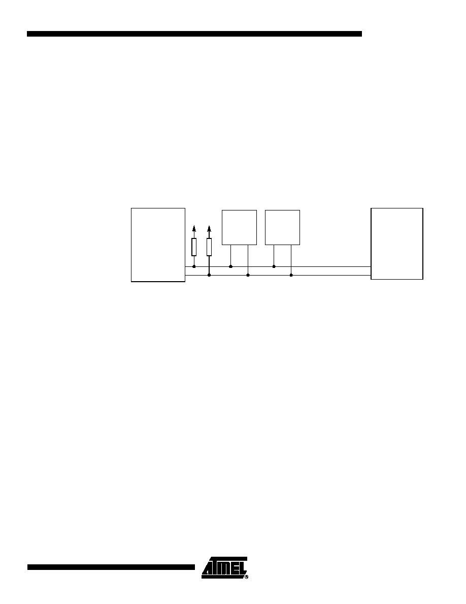
can be designed using this bus. Figure 20-1 shows a typical TWI bus configuration using the
AT89C5132 in master and slave modes. All the devices connected to the bus can be master and
slave.
Figure 20-1. Typical TWI Bus Configuration
20.1
Description
The CPU interfaces to the TWI logic via the following four 8-bit special function registers: the
Synchronous Serial Control register (SSCON SFR, see Table 26), the Synchronous Serial Data
register (SSDAT SFR, see Table 28), the Synchronous Serial Status register (SSSTA SFR, see
SSCON is used to enable the controller, to program the bit rate (see Table 26), to enable slave
modes, to acknowledge or not a received data, to send a START or a STOP condition on the
TWI bus, and to acknowledge a serial interrupt. A hardware reset disables the TWI controller.
SSSTA contains a status code which reflects the status of the TWI logic and the TWI bus. The
three least significant bits are always zero. The five most significant bits contains the status
code. There are 26 possible status codes. When SSSTA contains F8h, no relevant state infor-
mation is available and no serial interrupt is requested. A valid status code is available in SSSTA
after SSI is set by hardware and is still present until SSI has been reset by software. Table 20 to
Table 20-6 give the status for both master and slave modes and miscellaneous states.
SSDAT contains a Byte of serial data to be transmitted or a Byte which has just been received. It
is addressable while it is not in process of shifting a Byte. This occurs when TWI logic is in a
defined state and the serial interrupt flag is set. Data in SSDAT remains stable as long as SSI is
set. While data is being shifted out, data on the bus is simultaneously shifted in; SSDAT always
contains the last Byte present on the bus.
SSADR may be loaded with the 7 - bit slave address (7 most significant bits) to which the con-
troller will respond when programmed as a slave transmitter or receiver. The LSB is used to
enable general call address (00h) recognition.
Figure 20-2 shows how a data transfer is accomplished on the TWI bus.
AT89C5132
Master/Slave
LCD
Display
Audio
DAC
P1.6/SCL
P1.7/SDA
Rp
HOST
Microprocessor
SCL
SDA
相关PDF资料 |
PDF描述 |
|---|---|
| 202650-4 | PIN MODULE, 23 POSN, G-SERIES |
| 203959-5 | CONN RCPT 36POS VERT PANEL MT |
| 202651-2 | SKT MODULE, 23 POSN, G-SERIES |
| AT87C58X2-RLTUM | IC 8051 MCU 32K EPROM 44VQFP |
| AT87C58X2-RLTUL | IC 8051 MCU 32K EPROM 44VQFP |
相关代理商/技术参数 |
参数描述 |
|---|---|
| AT89C51-33AC | 功能描述:8位微控制器 -MCU Microcontroller RoHS:否 制造商:Silicon Labs 核心:8051 处理器系列:C8051F39x 数据总线宽度:8 bit 最大时钟频率:50 MHz 程序存储器大小:16 KB 数据 RAM 大小:1 KB 片上 ADC:Yes 工作电源电压:1.8 V to 3.6 V 工作温度范围:- 40 C to + 105 C 封装 / 箱体:QFN-20 安装风格:SMD/SMT |
| AT89C51-33AI | 功能描述:8位微控制器 -MCU Microcontroller RoHS:否 制造商:Silicon Labs 核心:8051 处理器系列:C8051F39x 数据总线宽度:8 bit 最大时钟频率:50 MHz 程序存储器大小:16 KB 数据 RAM 大小:1 KB 片上 ADC:Yes 工作电源电压:1.8 V to 3.6 V 工作温度范围:- 40 C to + 105 C 封装 / 箱体:QFN-20 安装风格:SMD/SMT |
| AT89C51-33JI | 功能描述:8位微控制器 -MCU Microcontroller RoHS:否 制造商:Silicon Labs 核心:8051 处理器系列:C8051F39x 数据总线宽度:8 bit 最大时钟频率:50 MHz 程序存储器大小:16 KB 数据 RAM 大小:1 KB 片上 ADC:Yes 工作电源电压:1.8 V to 3.6 V 工作温度范围:- 40 C to + 105 C 封装 / 箱体:QFN-20 安装风格:SMD/SMT |
| AT89C51-33PC | 功能描述:8位微控制器 -MCU Microcontroller RoHS:否 制造商:Silicon Labs 核心:8051 处理器系列:C8051F39x 数据总线宽度:8 bit 最大时钟频率:50 MHz 程序存储器大小:16 KB 数据 RAM 大小:1 KB 片上 ADC:Yes 工作电源电压:1.8 V to 3.6 V 工作温度范围:- 40 C to + 105 C 封装 / 箱体:QFN-20 安装风格:SMD/SMT |
| AT89C51-33PI | 功能描述:8位微控制器 -MCU Microcontroller RoHS:否 制造商:Silicon Labs 核心:8051 处理器系列:C8051F39x 数据总线宽度:8 bit 最大时钟频率:50 MHz 程序存储器大小:16 KB 数据 RAM 大小:1 KB 片上 ADC:Yes 工作电源电压:1.8 V to 3.6 V 工作温度范围:- 40 C to + 105 C 封装 / 箱体:QFN-20 安装风格:SMD/SMT |
发布紧急采购,3分钟左右您将得到回复。