参数资料
| 型号: | AT89C51CC03U-RDTIM |
| 厂商: | Atmel |
| 文件页数: | 38/198页 |
| 文件大小: | 0K |
| 描述: | IC 8051 MCU FLASH 64K 64VQFP |
| 标准包装: | 160 |
| 系列: | AT89C CAN |
| 核心处理器: | 8051 |
| 芯体尺寸: | 8-位 |
| 速度: | 40MHz |
| 连通性: | CAN,SPI,UART/USART |
| 外围设备: | POR,PWM,WDT |
| 输入/输出数: | 36 |
| 程序存储器容量: | 64KB(64K x 8) |
| 程序存储器类型: | 闪存 |
| EEPROM 大小: | 2K x 8 |
| RAM 容量: | 2.25K x 8 |
| 电压 - 电源 (Vcc/Vdd): | 3 V ~ 5.5 V |
| 数据转换器: | A/D 8x10b |
| 振荡器型: | 外部 |
| 工作温度: | -40°C ~ 85°C |
| 封装/外壳: | 44-LQFP |
| 包装: | 托盘 |
| 其它名称: | AT89C51CC03URDTIM |
第1页第2页第3页第4页第5页第6页第7页第8页第9页第10页第11页第12页第13页第14页第15页第16页第17页第18页第19页第20页第21页第22页第23页第24页第25页第26页第27页第28页第29页第30页第31页第32页第33页第34页第35页第36页第37页当前第38页第39页第40页第41页第42页第43页第44页第45页第46页第47页第48页第49页第50页第51页第52页第53页第54页第55页第56页第57页第58页第59页第60页第61页第62页第63页第64页第65页第66页第67页第68页第69页第70页第71页第72页第73页第74页第75页第76页第77页第78页第79页第80页第81页第82页第83页第84页第85页第86页第87页第88页第89页第90页第91页第92页第93页第94页第95页第96页第97页第98页第99页第100页第101页第102页第103页第104页第105页第106页第107页第108页第109页第110页第111页第112页第113页第114页第115页第116页第117页第118页第119页第120页第121页第122页第123页第124页第125页第126页第127页第128页第129页第130页第131页第132页第133页第134页第135页第136页第137页第138页第139页第140页第141页第142页第143页第144页第145页第146页第147页第148页第149页第150页第151页第152页第153页第154页第155页第156页第157页第158页第159页第160页第161页第162页第163页第164页第165页第166页第167页第168页第169页第170页第171页第172页第173页第174页第175页第176页第177页第178页第179页第180页第181页第182页第183页第184页第185页第186页第187页第188页第189页第190页第191页第192页第193页第194页第195页第196页第197页第198页
132
AT89C51CC03
4182O–CAN–09/08
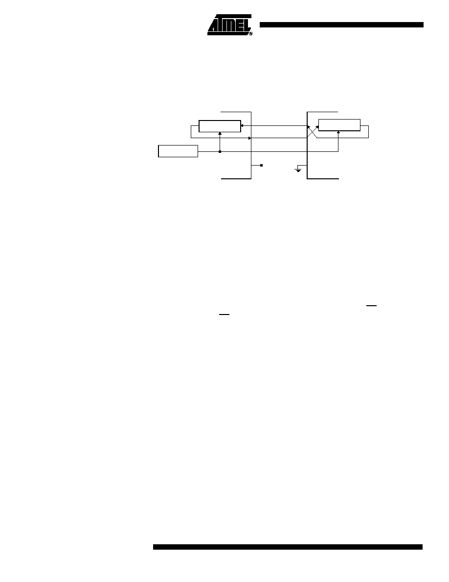
When the Master device transmits data to the Slave device via the MOSI line, the Slave
device responds by sending data to the Master device via the MISO line. This implies
full-duplex transmission with both data out and data in synchronized with the same clock
Figure 59. Full-Duplex Master-Slave Interconnection
Master Mode
The SPI operates in Master mode when the Master bit, MSTR (1), in the SPCON register
is set. Only one Master SPI device can initiate transmissions. Software begins the trans-
mission from a Master SPI Module by writing to the Serial Peripheral Data Register
(SPDAT). If the shift register is empty, the Byte is immediately transferred to the shift
register. The Byte begins shifting out on MOSI pin under the control of the serial clock,
SCK. Simultaneously, another Byte shifts in from the Slave on the Master’s MISO pin.
The transmission ends when the Serial Peripheral transfer data flag, SPIF, in SPSCR
becomes set. At the same time that SPIF becomes set, the received Byte from the Slave
is transferred to the receive data register in SPDAT. Software clears SPIF by reading
the Serial Peripheral Status register (SPSCR) with the SPIF bit set, and then reading the
SPDAT.
Slave Mode
The SPI operates in Slave mode when the Master bit, MSTR (2), in the SPCON register is
cleared. Before a data transmission occurs, the Slave Select pin, SS, of the Slave
device must be set to’0’. SS must remain low until the transmission is complete.
In a Slave SPI Module, data enters the shift register under the control of the SCK from
the Master SPI Module. After a Byte enters the shift register, it is immediately trans-
ferred to the receive data register in SPDAT, and the SPIF bit is set. To prevent an
overflow condition, Slave software must then read the SPDAT before another Byte
enters the shift register (3). A Slave SPI must complete the write to the SPDAT (shift reg-
ister) at least one bus cycle before the Master SPI starts a transmission. If the write to
the data register is late, the SPI transmits the data already in the shift register from the
previous transmission.
Transmission Formats
Software can select any of four combinations of serial clock (SCK) phase and polarity
using two bits in the SPCON: the Clock Polarity (CPOL (4)) and the Clock Phase
(CPHA4). CPOL defines the default SCK line level in idle state. It has no significant
effect on the transmission format. CPHA defines the edges on which the input data are
sampled and the edges on which the output data are shifted (Figure 60 and Figure 61).
The clock phase and polarity should be identical for the Master SPI device and the com-
municating Slave device.
8-bit Shift register
SPI
Clock Generator
Master MCU
8-bit Shift register
MISO
MOSI
SCK
VSS
VDD
SS
Slave MCU
1.
The SPI Module should be configured as a Master before it is enabled (SPEN set). Also,
the Master SPI should be configured before the Slave SPI.
2.
The SPI Module should be configured as a Slave before it is enabled (SPEN set).
3.
The maximum frequency of the SCK for an SPI configured as a Slave is the bus clock
speed.
4.
Before writing to the CPOL and CPHA bits, the SPI should be disabled (SPEN =’0’).
相关PDF资料 |
PDF描述 |
|---|---|
| AT89C51CC03U-7CTIM | IC 8051 MCU FLASH 64K 64BGA |
| AT89C51CC03C-S3SIM | IC 8051 MCU FLASH 64K 52PLCC |
| AT89C51CC03C-RLTIM | IC 8051 MCU FLASH 64K 44VQFP |
| AT89C51CC03C-7CTIM | IC 8051 MCU FLASH 64K 64BGA |
| AT89C5132-ROTIL | IC 8051 MCU FLASH 64K USB 80TQFP |
相关代理商/技术参数 |
参数描述 |
|---|---|
| AT89C51CC03U-RLRIM | 功能描述:IC 8051 MCU FLASH 64K 44VQFP RoHS:否 类别:集成电路 (IC) >> 嵌入式 - 微控制器, 系列:AT89C CAN 标准包装:1,500 系列:AVR® ATtiny 核心处理器:AVR 芯体尺寸:8-位 速度:16MHz 连通性:I²C,LIN,SPI,UART/USART,USI 外围设备:欠压检测/复位,POR,PWM,温度传感器,WDT 输入/输出数:16 程序存储器容量:8KB(4K x 16) 程序存储器类型:闪存 EEPROM 大小:512 x 8 RAM 容量:512 x 8 电压 - 电源 (Vcc/Vdd):2.7 V ~ 5.5 V 数据转换器:A/D 11x10b 振荡器型:内部 工作温度:-40°C ~ 125°C 封装/外壳:20-SOIC(0.295",7.50mm 宽) 包装:带卷 (TR) |
| AT89C51CC03U-RLTIM | 功能描述:IC 8051 MCU FLASH 64K 44VQFP RoHS:否 类别:集成电路 (IC) >> 嵌入式 - 微控制器, 系列:AT89C CAN 标准包装:9 系列:87C 核心处理器:8051 芯体尺寸:8-位 速度:40/20MHz 连通性:UART/USART 外围设备:POR,WDT 输入/输出数:32 程序存储器容量:32KB(32K x 8) 程序存储器类型:OTP EEPROM 大小:- RAM 容量:256 x 8 电压 - 电源 (Vcc/Vdd):4.5 V ~ 5.5 V 数据转换器:- 振荡器型:内部 工作温度:0°C ~ 70°C 封装/外壳:40-DIP(0.600",15.24mm) 包装:管件 |
| AT89C51CC03U-S3RIM | 功能描述:IC 8051 MCU FLASH 64K 52PLCC RoHS:否 类别:集成电路 (IC) >> 嵌入式 - 微控制器, 系列:AT89C CAN 标准包装:1,500 系列:AVR® ATtiny 核心处理器:AVR 芯体尺寸:8-位 速度:16MHz 连通性:I²C,LIN,SPI,UART/USART,USI 外围设备:欠压检测/复位,POR,PWM,温度传感器,WDT 输入/输出数:16 程序存储器容量:8KB(4K x 16) 程序存储器类型:闪存 EEPROM 大小:512 x 8 RAM 容量:512 x 8 电压 - 电源 (Vcc/Vdd):2.7 V ~ 5.5 V 数据转换器:A/D 11x10b 振荡器型:内部 工作温度:-40°C ~ 125°C 封装/外壳:20-SOIC(0.295",7.50mm 宽) 包装:带卷 (TR) |
| AT89C51CC03U-S3SIM | 制造商:Atmel Corporation 功能描述:MCU 8-bit AT89 80C51 CISC 64KB Flash 5V 52-Pin PLCC Stick |
| AT89C51CC03U-SLRIM | 功能描述:IC 8051 MCU FLASH 64K 44PLCC RoHS:否 类别:集成电路 (IC) >> 嵌入式 - 微控制器, 系列:AT89C CAN 标准包装:1,500 系列:AVR® ATtiny 核心处理器:AVR 芯体尺寸:8-位 速度:16MHz 连通性:I²C,LIN,SPI,UART/USART,USI 外围设备:欠压检测/复位,POR,PWM,温度传感器,WDT 输入/输出数:16 程序存储器容量:8KB(4K x 16) 程序存储器类型:闪存 EEPROM 大小:512 x 8 RAM 容量:512 x 8 电压 - 电源 (Vcc/Vdd):2.7 V ~ 5.5 V 数据转换器:A/D 11x10b 振荡器型:内部 工作温度:-40°C ~ 125°C 封装/外壳:20-SOIC(0.295",7.50mm 宽) 包装:带卷 (TR) |
发布紧急采购,3分钟左右您将得到回复。