- 您现在的位置:买卖IC网 > PDF目录12048 > AT89C51IC2-RLTUL (Atmel)IC 8051 MCU FLASH 32K 44VQFP PDF资料下载
参数资料
| 型号: | AT89C51IC2-RLTUL |
| 厂商: | Atmel |
| 文件页数: | 55/140页 |
| 文件大小: | 0K |
| 描述: | IC 8051 MCU FLASH 32K 44VQFP |
| 产品培训模块: | MCU Product Line Introduction |
| 标准包装: | 800 |
| 系列: | 89C |
| 核心处理器: | 8051 |
| 芯体尺寸: | 8-位 |
| 速度: | 60MHz |
| 连通性: | I²C,SPI,UART/USART |
| 外围设备: | POR,PWM,WDT |
| 输入/输出数: | 34 |
| 程序存储器容量: | 32KB(32K x 8) |
| 程序存储器类型: | 闪存 |
| RAM 容量: | 1.25K x 8 |
| 电压 - 电源 (Vcc/Vdd): | 2.7 V ~ 3.6 V |
| 振荡器型: | 外部 |
| 工作温度: | -40°C ~ 85°C |
| 封装/外壳: | 44-LQFP |
| 包装: | 托盘 |
| 配用: | AT89OCD-01-ND - USB EMULATOR FOR AT8XC51 MCU |
第1页第2页第3页第4页第5页第6页第7页第8页第9页第10页第11页第12页第13页第14页第15页第16页第17页第18页第19页第20页第21页第22页第23页第24页第25页第26页第27页第28页第29页第30页第31页第32页第33页第34页第35页第36页第37页第38页第39页第40页第41页第42页第43页第44页第45页第46页第47页第48页第49页第50页第51页第52页第53页第54页当前第55页第56页第57页第58页第59页第60页第61页第62页第63页第64页第65页第66页第67页第68页第69页第70页第71页第72页第73页第74页第75页第76页第77页第78页第79页第80页第81页第82页第83页第84页第85页第86页第87页第88页第89页第90页第91页第92页第93页第94页第95页第96页第97页第98页第99页第100页第101页第102页第103页第104页第105页第106页第107页第108页第109页第110页第111页第112页第113页第114页第115页第116页第117页第118页第119页第120页第121页第122页第123页第124页第125页第126页第127页第128页第129页第130页第131页第132页第133页第134页第135页第136页第137页第138页第139页第140页
21
AT89C51IC2
4301D–8051–02/08
Enhanced Features
In comparison to the original 80C52, the AT89C51IC2 implements some new features,
which are:
The X2 option
The Dual Data Pointer
The extended RAM
The Programmable Counter Array (PCA)
The Hardware Watchdog
The SPI interface
The 2-wire interface
The 4 level interrupt priority system
The power-off flag
The Power On Reset
The ONCE mode
The ALE disabling
Some enhanced features are also located in the UART and the timer 2
X2 Feature and OSCA
Clock Generation
The AT89C51IC2 core needs only 6 clock periods per machine cycle. This feature
called ”X2” provides the following advantages:
Divide frequency crystals by 2 (cheaper crystals) while keeping same CPU power.
Save power consumption while keeping same CPU power (oscillator power saving).
Save power consumption by dividing dynamically the operating frequency by 2 in
operating and idle modes.
Increase CPU power by 2 while keeping same crystal frequency.
In order to keep the original C51 compatibility, a divider by 2 is inserted between the
XTALA1 signal and the main clock input of the core (phase generator). This divider may
be disabled by software.
Description
The clock for the whole circuit and peripherals is first divided by two before being used
by the CPU core and the peripherals.
This allows any cyclic ratio to be accepted on XTALA1 input. In X2 mode, as this divider
is bypassed, the signals on XTALA1 must have a cyclic ratio between 40 to 60%.
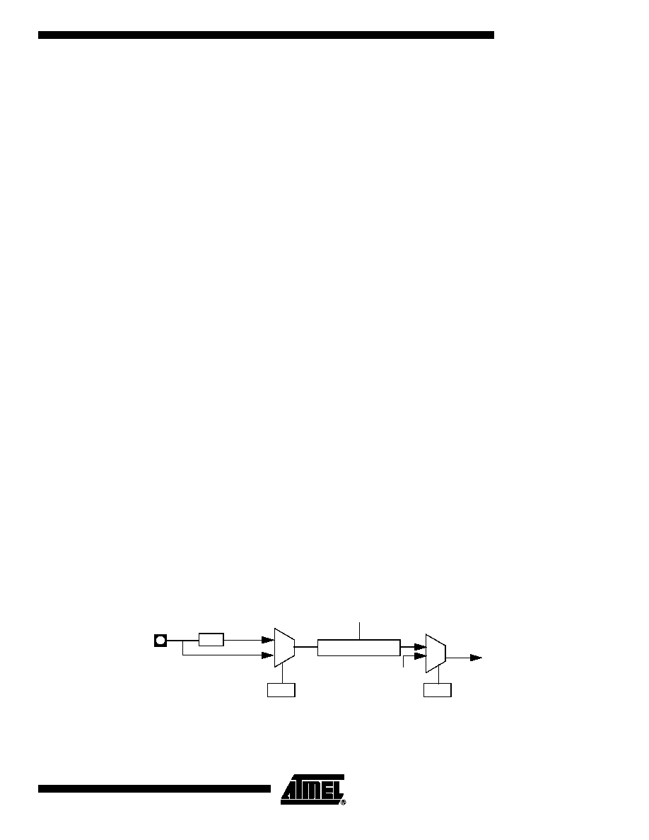
Figure 5. shows the clock generation block diagram.x2 bit is validated on the rising edge
of the XTALA1÷2 to avoid glitches when switching from X2 to STD mode. Figure 6.
shows the switching mode waveforms.
Figure 5. Clock Generation Diagram
XTALA1
2
CKCON0
X2
8 bit Prescaler
F
OSCA
F
XTAL
XTALA1:2
F
CLK CPU
F
CLK PERIPH
CKSEL
CKS
F
OSCB
CKRL
0
1
0
1
相关PDF资料 |
PDF描述 |
|---|---|
| 860267-4 | CONN PLUG 6POS LGH 24-20AWG |
| VJ2220Y562KBFAT4X | CAP CER 5600PF 2KV 10% X7R 2220 |
| VE-J33-IX-B1 | CONVERTER MOD DC/DC 24V 75W |
| VJ2220Y822KBFAT4X | CAP CER 8200PF 2KV 10% X7R 2220 |
| AT89C51IC2-RLTIL | IC 8051 MCU FLASH 32K 44VQFP |
相关代理商/技术参数 |
参数描述 |
|---|---|
| AT89C51IC2-RLTUM | 功能描述:8位微控制器 -MCU C51IC2 32K FLASH I2C 32KHz 5V RoHS:否 制造商:Silicon Labs 核心:8051 处理器系列:C8051F39x 数据总线宽度:8 bit 最大时钟频率:50 MHz 程序存储器大小:16 KB 数据 RAM 大小:1 KB 片上 ADC:Yes 工作电源电压:1.8 V to 3.6 V 工作温度范围:- 40 C to + 105 C 封装 / 箱体:QFN-20 安装风格:SMD/SMT |
| AT89C51IC2-SLRIL | 功能描述:IC MCU FLASH 8051 32K 3V 44-PLCC RoHS:否 类别:集成电路 (IC) >> 嵌入式 - 微控制器, 系列:89C 标准包装:1,500 系列:AVR® ATtiny 核心处理器:AVR 芯体尺寸:8-位 速度:16MHz 连通性:I²C,LIN,SPI,UART/USART,USI 外围设备:欠压检测/复位,POR,PWM,温度传感器,WDT 输入/输出数:16 程序存储器容量:8KB(4K x 16) 程序存储器类型:闪存 EEPROM 大小:512 x 8 RAM 容量:512 x 8 电压 - 电源 (Vcc/Vdd):2.7 V ~ 5.5 V 数据转换器:A/D 11x10b 振荡器型:内部 工作温度:-40°C ~ 125°C 封装/外壳:20-SOIC(0.295",7.50mm 宽) 包装:带卷 (TR) |
| AT89C51IC2-SLRIM | 功能描述:IC MCU FLASH 8051 32K 5V 44-PLCC RoHS:否 类别:集成电路 (IC) >> 嵌入式 - 微控制器, 系列:89C 标准包装:1,500 系列:AVR® ATtiny 核心处理器:AVR 芯体尺寸:8-位 速度:16MHz 连通性:I²C,LIN,SPI,UART/USART,USI 外围设备:欠压检测/复位,POR,PWM,温度传感器,WDT 输入/输出数:16 程序存储器容量:8KB(4K x 16) 程序存储器类型:闪存 EEPROM 大小:512 x 8 RAM 容量:512 x 8 电压 - 电源 (Vcc/Vdd):2.7 V ~ 5.5 V 数据转换器:A/D 11x10b 振荡器型:内部 工作温度:-40°C ~ 125°C 封装/外壳:20-SOIC(0.295",7.50mm 宽) 包装:带卷 (TR) |
| AT89C51IC2-SLRUL | 功能描述:8位微控制器 -MCU C51IC2 32K FLASH I2C 32KHz 3V RoHS:否 制造商:Silicon Labs 核心:8051 处理器系列:C8051F39x 数据总线宽度:8 bit 最大时钟频率:50 MHz 程序存储器大小:16 KB 数据 RAM 大小:1 KB 片上 ADC:Yes 工作电源电压:1.8 V to 3.6 V 工作温度范围:- 40 C to + 105 C 封装 / 箱体:QFN-20 安装风格:SMD/SMT |
| AT89C51IC2-SLRUM | 功能描述:8位微控制器 -MCU C51IC2 32K FLASH I2C 32KHz 5V RoHS:否 制造商:Silicon Labs 核心:8051 处理器系列:C8051F39x 数据总线宽度:8 bit 最大时钟频率:50 MHz 程序存储器大小:16 KB 数据 RAM 大小:1 KB 片上 ADC:Yes 工作电源电压:1.8 V to 3.6 V 工作温度范围:- 40 C to + 105 C 封装 / 箱体:QFN-20 安装风格:SMD/SMT |
发布紧急采购,3分钟左右您将得到回复。