- 您现在的位置:买卖IC网 > PDF目录11795 > AT89C51ID2-RLRUM (Atmel)IC 8051 MCU 64K FLASH 44-VQFP PDF资料下载
参数资料
| 型号: | AT89C51ID2-RLRUM |
| 厂商: | Atmel |
| 文件页数: | 21/157页 |
| 文件大小: | 0K |
| 描述: | IC 8051 MCU 64K FLASH 44-VQFP |
| 产品培训模块: | MCU Product Line Introduction |
| 标准包装: | 1,500 |
| 系列: | 89C |
| 核心处理器: | 8051 |
| 芯体尺寸: | 8-位 |
| 速度: | 60MHz |
| 连通性: | I²C,SPI,UART/USART |
| 外围设备: | POR,PWM,WDT |
| 输入/输出数: | 34 |
| 程序存储器容量: | 64KB(64K x 8) |
| 程序存储器类型: | 闪存 |
| EEPROM 大小: | 2K x 8 |
| RAM 容量: | 2K x 8 |
| 电压 - 电源 (Vcc/Vdd): | 2.7 V ~ 5.5 V |
| 振荡器型: | 外部 |
| 工作温度: | -40°C ~ 85°C |
| 封装/外壳: | 44-LQFP |
| 包装: | 标准包装 |
| 配用: | AT89OCD-01-ND - USB EMULATOR FOR AT8XC51 MCU |
| 其它名称: | AT89C51ID2-RLRUMDKR |
第1页第2页第3页第4页第5页第6页第7页第8页第9页第10页第11页第12页第13页第14页第15页第16页第17页第18页第19页第20页当前第21页第22页第23页第24页第25页第26页第27页第28页第29页第30页第31页第32页第33页第34页第35页第36页第37页第38页第39页第40页第41页第42页第43页第44页第45页第46页第47页第48页第49页第50页第51页第52页第53页第54页第55页第56页第57页第58页第59页第60页第61页第62页第63页第64页第65页第66页第67页第68页第69页第70页第71页第72页第73页第74页第75页第76页第77页第78页第79页第80页第81页第82页第83页第84页第85页第86页第87页第88页第89页第90页第91页第92页第93页第94页第95页第96页第97页第98页第99页第100页第101页第102页第103页第104页第105页第106页第107页第108页第109页第110页第111页第112页第113页第114页第115页第116页第117页第118页第119页第120页第121页第122页第123页第124页第125页第126页第127页第128页第129页第130页第131页第132页第133页第134页第135页第136页第137页第138页第139页第140页第141页第142页第143页第144页第145页第146页第147页第148页第149页第150页第151页第152页第153页第154页第155页第156页第157页
117
AT89C51ID2
4289C–8051–11/05
Flash Registers and
Memory Map
The AT89C51ID2 Flash memory uses several registers for his management:
Hardware registers can only be accessed through the parallel programming modes
which are handled by the parallel programmer.
Software registers are in a special page of the Flash memory which can be
accessed through the API or with the parallel programming modes. This page,
called "Extra Flash Memory", is not in the internal Flash program memory
addressing space.
Hardware Register
The only hardware register of the AT89C51ID2 is called Hardware Security Byte (HSB).
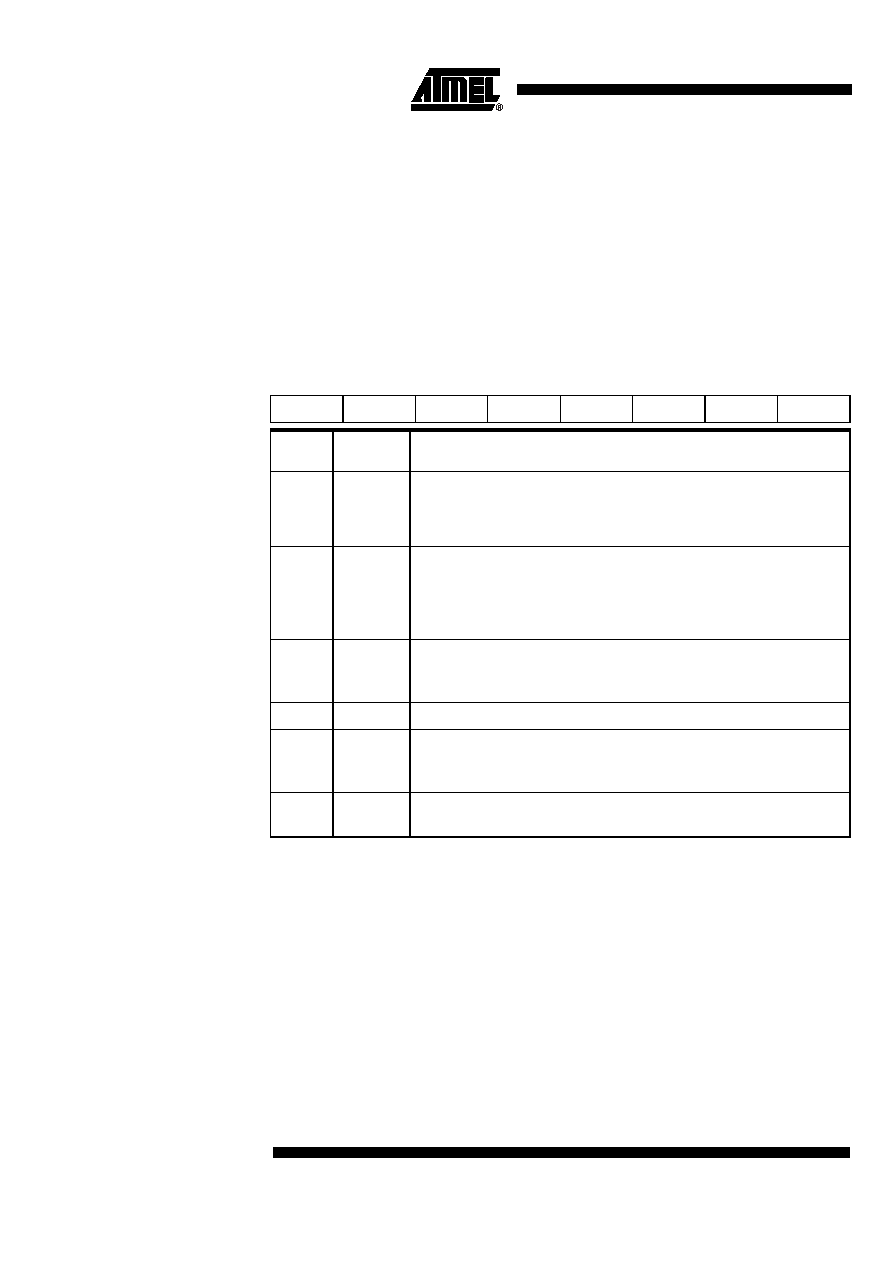
Table 88. Hardware Security Byte (HSB)
Boot Loader Jump Bit (BLJB)
One bit of the HSB, the BLJB bit, is used to force the boot address:
When this bit is programmed (‘1’ value) the boot address is 0000h.
When this bit is unprogrammed (‘1’ value) the boot address is F800h. By default,
this bit is unprogrammed and the ISP is enabled.
Flash Memory Lock Bits
The three lock bits provide different levels of protection for the on-chip code and data,
when programmed as shown in Table 89.
76
543
210
X2
BLJB
OSC
-
XRAM
LB2
LB1
LB0
Bit
Number
Bit
Mnemonic
Description
7X2
X2 Mode
Programmed (‘0’ value) to force X2 mode (6 clocks per instruction) after reset.
Unprogrammed (‘1’ Value) to force X1 mode, Standard Mode, after reset
(Default).
6BLJB
Boot Loader Jump Bit
Unprogrammed (‘1’ value) to start the user’s application on next reset at address
0000h.
Programmed (‘0’ value) to start the boot loader at address F800h on next reset
(Default).
5OSC
Oscillator Bit
Programmed to allow oscillator B at startup
Unprogrammed this bit to allow oscillator A at startup ( Default).
4-
Reserved
3XRAM
XRAM config bit (only programmable by programmer tools)
Programmed to inhibit XRAM
Unprogrammed, this bit to valid XRAM (Default)
2-0
LB2-0
User Memory Lock Bits (only programmable by programmer tools)
See Table 89
相关PDF资料 |
PDF描述 |
|---|---|
| AT32UC3A364-ALUR | IC MCU 64KB FLASH 144LQFP |
| DS80C310+FCG | IC MCU HI SPEED 25MHZ 44-MQFP |
| D38999/20WD5SN | CONN RCPT 5POS WALL MNT W/SCKT |
| ATMEGA6490-16AUR | MCU AVR 64KB FLASH 16MHZ 64TQFP |
| D38999/20FD5SN | CONN RCPT 5POS WALL MNT W/SCKT |
相关代理商/技术参数 |
参数描述 |
|---|---|
| AT89C51ID2-RLTIM | 功能描述:IC 8051 MCU FLASH 64K 44VQFP RoHS:否 类别:集成电路 (IC) >> 嵌入式 - 微控制器, 系列:89C 标准包装:9 系列:87C 核心处理器:8051 芯体尺寸:8-位 速度:40/20MHz 连通性:UART/USART 外围设备:POR,WDT 输入/输出数:32 程序存储器容量:32KB(32K x 8) 程序存储器类型:OTP EEPROM 大小:- RAM 容量:256 x 8 电压 - 电源 (Vcc/Vdd):4.5 V ~ 5.5 V 数据转换器:- 振荡器型:内部 工作温度:0°C ~ 70°C 封装/外壳:40-DIP(0.600",15.24mm) 包装:管件 |
| AT89C51ID2-RLTUM | 功能描述:8位微控制器 -MCU C51ID2 64K FLASH 32KHz 3-5.5V RoHS:否 制造商:Silicon Labs 核心:8051 处理器系列:C8051F39x 数据总线宽度:8 bit 最大时钟频率:50 MHz 程序存储器大小:16 KB 数据 RAM 大小:1 KB 片上 ADC:Yes 工作电源电压:1.8 V to 3.6 V 工作温度范围:- 40 C to + 105 C 封装 / 箱体:QFN-20 安装风格:SMD/SMT |
| AT89C51ID2-SLRIM | 功能描述:IC MCU FLASH 8051 64K 5V 44-PLCC RoHS:否 类别:集成电路 (IC) >> 嵌入式 - 微控制器, 系列:89C 标准包装:1,500 系列:AVR® ATtiny 核心处理器:AVR 芯体尺寸:8-位 速度:16MHz 连通性:I²C,LIN,SPI,UART/USART,USI 外围设备:欠压检测/复位,POR,PWM,温度传感器,WDT 输入/输出数:16 程序存储器容量:8KB(4K x 16) 程序存储器类型:闪存 EEPROM 大小:512 x 8 RAM 容量:512 x 8 电压 - 电源 (Vcc/Vdd):2.7 V ~ 5.5 V 数据转换器:A/D 11x10b 振荡器型:内部 工作温度:-40°C ~ 125°C 封装/外壳:20-SOIC(0.295",7.50mm 宽) 包装:带卷 (TR) |
| AT89C51ID2-SLRUM | 功能描述:8位微控制器 -MCU C51ID2 64K FLASH TWI 32KHz 5V RoHS:否 制造商:Silicon Labs 核心:8051 处理器系列:C8051F39x 数据总线宽度:8 bit 最大时钟频率:50 MHz 程序存储器大小:16 KB 数据 RAM 大小:1 KB 片上 ADC:Yes 工作电源电压:1.8 V to 3.6 V 工作温度范围:- 40 C to + 105 C 封装 / 箱体:QFN-20 安装风格:SMD/SMT |
| AT89C51ID2-SLSIM | 制造商:ATMEL 制造商全称:ATMEL Corporation 功能描述:8-bit Flash Microcontroller |
发布紧急采购,3分钟左右您将得到回复。