- 您现在的位置:买卖IC网 > PDF目录12052 > AT89LP3240-20AU (Atmel)MCU 8051 32K FLASH 20MHZ PDF资料下载
参数资料
| 型号: | AT89LP3240-20AU |
| 厂商: | Atmel |
| 文件页数: | 72/200页 |
| 文件大小: | 0K |
| 描述: | MCU 8051 32K FLASH 20MHZ |
| 标准包装: | 160 |
| 系列: | 89LP |
| 核心处理器: | 8051 |
| 芯体尺寸: | 8-位 |
| 速度: | 20MHz |
| 连通性: | I²C,SPI,UART/USART |
| 外围设备: | 欠压检测/复位,POR,PWM,WDT |
| 输入/输出数: | 38 |
| 程序存储器容量: | 32KB(32K x 8) |
| 程序存储器类型: | 闪存 |
| EEPROM 大小: | 8K x 8 |
| RAM 容量: | 4.25K x 8 |
| 电压 - 电源 (Vcc/Vdd): | 2.4 V ~ 3.6 V |
| 数据转换器: | A/D 8x10b |
| 振荡器型: | 内部 |
| 工作温度: | -40°C ~ 85°C |
| 封装/外壳: | 44-TQFP |
| 包装: | 托盘 |
第1页第2页第3页第4页第5页第6页第7页第8页第9页第10页第11页第12页第13页第14页第15页第16页第17页第18页第19页第20页第21页第22页第23页第24页第25页第26页第27页第28页第29页第30页第31页第32页第33页第34页第35页第36页第37页第38页第39页第40页第41页第42页第43页第44页第45页第46页第47页第48页第49页第50页第51页第52页第53页第54页第55页第56页第57页第58页第59页第60页第61页第62页第63页第64页第65页第66页第67页第68页第69页第70页第71页当前第72页第73页第74页第75页第76页第77页第78页第79页第80页第81页第82页第83页第84页第85页第86页第87页第88页第89页第90页第91页第92页第93页第94页第95页第96页第97页第98页第99页第100页第101页第102页第103页第104页第105页第106页第107页第108页第109页第110页第111页第112页第113页第114页第115页第116页第117页第118页第119页第120页第121页第122页第123页第124页第125页第126页第127页第128页第129页第130页第131页第132页第133页第134页第135页第136页第137页第138页第139页第140页第141页第142页第143页第144页第145页第146页第147页第148页第149页第150页第151页第152页第153页第154页第155页第156页第157页第158页第159页第160页第161页第162页第163页第164页第165页第166页第167页第168页第169页第170页第171页第172页第173页第174页第175页第176页第177页第178页第179页第180页第181页第182页第183页第184页第185页第186页第187页第188页第189页第190页第191页第192页第193页第194页第195页第196页第197页第198页第199页第200页
163
3706C–MICRO–2/11
AT89LP3240/6440
25.4
Status Register
The current state of the memory may be accessed by reading the status register. The status reg-
ister is shown in Table 25-3.
25.5
DATA Polling
The AT89LP3240/6440 implements DATA polling to indicate the end of a programming cycle.
While the device is busy, any attempted read of the last byte written will return the data byte with
the MSB complemented. Once the programming cycle has completed, the true value will be
accessible. During Erase the data is assumed to be FFH and DATA polling will return 7FH.
When writing multiple bytes in a page, the DATA value will be the last data byte loaded before
programming begins, not the written byte with the highest physical address within the page.
25.6
Flash Security
The AT89LP3240/6440 provides two Lock Bits for Flash Code and Data Memory security. Lock
bits can be left unprogrammed (FFh) or programmed (00h) to obtain the protection levels listed
in Table 25-4. Lock bits can only be erased (set to FFh) by Chip Erase. Lock bit mode 2 disables
programming of all memory spaces, including the User Signature Array and User Configuration
Fuses. User fuses must be programmed before enabling Lock bit mode 2 or 3. Lock bit mode 3
implements mode 2 and also blocks reads from the code and data memories; however, reads of
the User Signature Array, Atmel Signature Array, and User Configuration Fuses are still allowed.
The Lock Bits will not disable FDATA or IAP programming initiated by the application software.
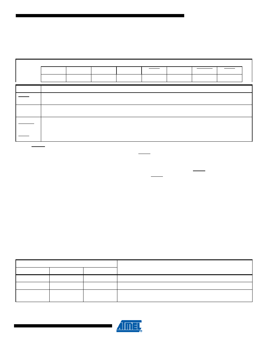
Table 25-3.
Status
Register
–
––
–
LOAD
SUCCESS
WRTINH
BUSY
Bit
7
6
543
21
0
Symbol
Function
LOAD
Load flag. Cleared low by the load page buffer command and set high by the next memory write. This flag signals that
the page buffer was previously loaded with data by the load page buffer command.
SUCCESS
Success flag. Cleared low at the start of a programming cycle and will only be set high if the programming cycle
completes without interruption from the brownout detector.
WRTINH
Write Inhibit flag. Cleared low by the brownout detector (BOD) whenever programming is inhibited due to VDD falling
below the minimum required programming voltage. If a BOD episode occurs during programming, the SUCCESS flag
will remain low after the cycle is complete.
BUSY
Busy flag. Cleared low whenever the memory is busy programming or if write is currently inhibited.
Table 25-4.
Lock Bit Protection Modes
Program Lock Bits (by address)
Mode
00h
01h
Protection Mode
1
FFh
No program lock features
200h
FFh
Further programming of the Flash is disabled
3
00h
Further programming of the Flash is disabled and verify (read) is also
disabled; OCD is disabled
相关PDF资料 |
PDF描述 |
|---|---|
| VE-J02-IY-F1 | CONVERTER MOD DC/DC 15V 50W |
| VI-J0L-IX-B1 | CONVERTER MOD DC/DC 28V 75W |
| VE-J01-IY-F2 | CONVERTER MOD DC/DC 12V 50W |
| AT89LP3240-20JU | MCU 8051 32K FLASH 20MHZ |
| AT89LP3240-20PU | MCU 8051 32K FLASH 20MHZ |
相关代理商/技术参数 |
参数描述 |
|---|---|
| AT89LP3240-20JU | 功能描述:8位微控制器 -MCU Sngl-Cycle 8051 IND 2.4-3.6V 32K ISP FL RoHS:否 制造商:Silicon Labs 核心:8051 处理器系列:C8051F39x 数据总线宽度:8 bit 最大时钟频率:50 MHz 程序存储器大小:16 KB 数据 RAM 大小:1 KB 片上 ADC:Yes 工作电源电压:1.8 V to 3.6 V 工作温度范围:- 40 C to + 105 C 封装 / 箱体:QFN-20 安装风格:SMD/SMT |
| AT89LP3240-20MU | 功能描述:8位微控制器 -MCU Sngl-Cycle 8051 IND 2.4-3.6V 32K ISP FL RoHS:否 制造商:Silicon Labs 核心:8051 处理器系列:C8051F39x 数据总线宽度:8 bit 最大时钟频率:50 MHz 程序存储器大小:16 KB 数据 RAM 大小:1 KB 片上 ADC:Yes 工作电源电压:1.8 V to 3.6 V 工作温度范围:- 40 C to + 105 C 封装 / 箱体:QFN-20 安装风格:SMD/SMT |
| AT89LP3240-20PU | 功能描述:8位微控制器 -MCU Sngl-Cycle 8051 IND 2.4-3.6V 32K ISP FL RoHS:否 制造商:Silicon Labs 核心:8051 处理器系列:C8051F39x 数据总线宽度:8 bit 最大时钟频率:50 MHz 程序存储器大小:16 KB 数据 RAM 大小:1 KB 片上 ADC:Yes 工作电源电压:1.8 V to 3.6 V 工作温度范围:- 40 C to + 105 C 封装 / 箱体:QFN-20 安装风格:SMD/SMT |
| AT89LP4052-16PI | 功能描述:8位微控制器 -MCU Microcontroller RoHS:否 制造商:Silicon Labs 核心:8051 处理器系列:C8051F39x 数据总线宽度:8 bit 最大时钟频率:50 MHz 程序存储器大小:16 KB 数据 RAM 大小:1 KB 片上 ADC:Yes 工作电源电压:1.8 V to 3.6 V 工作温度范围:- 40 C to + 105 C 封装 / 箱体:QFN-20 安装风格:SMD/SMT |
| AT89LP4052-16PU | 功能描述:8位微控制器 -MCU Microcontroller RoHS:否 制造商:Silicon Labs 核心:8051 处理器系列:C8051F39x 数据总线宽度:8 bit 最大时钟频率:50 MHz 程序存储器大小:16 KB 数据 RAM 大小:1 KB 片上 ADC:Yes 工作电源电压:1.8 V to 3.6 V 工作温度范围:- 40 C to + 105 C 封装 / 箱体:QFN-20 安装风格:SMD/SMT |
发布紧急采购,3分钟左右您将得到回复。