- 您现在的位置:买卖IC网 > PDF目录12052 > AT89LP3240-20JU (Atmel)MCU 8051 32K FLASH 20MHZ PDF资料下载
参数资料
| 型号: | AT89LP3240-20JU |
| 厂商: | Atmel |
| 文件页数: | 200/200页 |
| 文件大小: | 0K |
| 描述: | MCU 8051 32K FLASH 20MHZ |
| 标准包装: | 27 |
| 系列: | 89LP |
| 核心处理器: | 8051 |
| 芯体尺寸: | 8-位 |
| 速度: | 20MHz |
| 连通性: | I²C,SPI,UART/USART |
| 外围设备: | 欠压检测/复位,POR,PWM,WDT |
| 输入/输出数: | 38 |
| 程序存储器容量: | 32KB(32K x 8) |
| 程序存储器类型: | 闪存 |
| EEPROM 大小: | 8K x 8 |
| RAM 容量: | 4.25K x 8 |
| 电压 - 电源 (Vcc/Vdd): | 2.4 V ~ 3.6 V |
| 数据转换器: | A/D 8x10b |
| 振荡器型: | 内部 |
| 工作温度: | -40°C ~ 85°C |
| 封装/外壳: | 44-LCC(J 形引线) |
| 包装: | 管件 |
第1页第2页第3页第4页第5页第6页第7页第8页第9页第10页第11页第12页第13页第14页第15页第16页第17页第18页第19页第20页第21页第22页第23页第24页第25页第26页第27页第28页第29页第30页第31页第32页第33页第34页第35页第36页第37页第38页第39页第40页第41页第42页第43页第44页第45页第46页第47页第48页第49页第50页第51页第52页第53页第54页第55页第56页第57页第58页第59页第60页第61页第62页第63页第64页第65页第66页第67页第68页第69页第70页第71页第72页第73页第74页第75页第76页第77页第78页第79页第80页第81页第82页第83页第84页第85页第86页第87页第88页第89页第90页第91页第92页第93页第94页第95页第96页第97页第98页第99页第100页第101页第102页第103页第104页第105页第106页第107页第108页第109页第110页第111页第112页第113页第114页第115页第116页第117页第118页第119页第120页第121页第122页第123页第124页第125页第126页第127页第128页第129页第130页第131页第132页第133页第134页第135页第136页第137页第138页第139页第140页第141页第142页第143页第144页第145页第146页第147页第148页第149页第150页第151页第152页第153页第154页第155页第156页第157页第158页第159页第160页第161页第162页第163页第164页第165页第166页第167页第168页第169页第170页第171页第172页第173页第174页第175页第176页第177页第178页第179页第180页第181页第182页第183页第184页第185页第186页第187页第188页第189页第190页第191页第192页第193页第194页第195页第196页第197页第198页第199页当前第200页
99
3706C–MICRO–2/11
AT89LP3240/6440
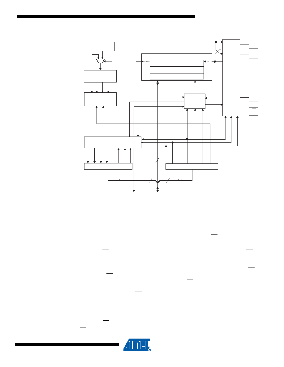
Figure 17-1. SPI Block Diagram
The interconnection between master and slave CPUs with SPI is shown in Figure 17-2. The four
pins in the interface are Master-In/Slave-Out (MISO), Master-Out/Slave-In (MOSI), Shift Clock
(SCK), and Slave Select (SS). The SCK pin is the clock output in master mode, but is the clock
input in slave mode. The MSTR bit in SPCR determines the directions of MISO and MOSI. Also
notice that MOSI connects to MOSI and MISO to MISO. By default SS/P1.4 is an input to both
master and slave devices.
In slave mode, SS must be driven low to select an individual device as a slave. When SS is held
low, the SPI is activated, and MISO becomes an output if configured so by the user. All other
pins are inputs. When SS is driven high, all pins are inputs, and the SPI is passive, which means
that it will not receive incoming data. Note that the SPI logic will be reset once the SS pin is
driven high. The SS pin is useful for packet/byte synchronization to keep the slave bit counter
synchronous with the master clock generator. When the SS pin is driven high, the SPI slave will
immediately reset the send and receive logic, and drop any partially received data in the Shift
Register.The slave may ignore SS by setting its SSIG bit in SPSR. When SSIG = 1, the slave is
always enabled and operates in 3-wire mode. However, the slave output on MISO may still be
disabled by setting DISSO=1.
The In-System Programming (ISP) interface also uses the SPI pins. Although the ISP protocol is
SPI-based, the SS pin has special meaning and must be driven by the master as a frame delim-
iter. SS cannot be tied to ground for ISP to function correctly.
Oscillator
8-bit Shift Register
Read Data Buffer
Pin
Control
Logic
SPI Control
SPI Status Register
SPI Interrupt
Request
Internal
Data Bus
Select
SPI Clock (Master)
Divider
÷4/÷8/÷32/÷64
SPI Control Register
8
SPIF
WCOL
SPR1
MSTR
TSCK
Clock
Logic
MSB
S
M
SPE
DORD
MSTR
CPOL
CPHA
SPR1
SPR0
MSTR
SPE
DORD
LSB
S
M
S
MISO
P1.6
MOSI
P1.5
SCK
1.7
SS
P1.4
SPR0
SPE
Write Data Buffer
MODF
TXE
ENH
TSCK
0
1
T1 OVF
DISSO
SSIG
相关PDF资料 |
PDF描述 |
|---|---|
| AT89LP3240-20PU | MCU 8051 32K FLASH 20MHZ |
| VI-JTZ-IY-F4 | CONVERTER MOD DC/DC 2V 20W |
| VI-JTZ-IY-F2 | CONVERTER MOD DC/DC 2V 20W |
| ATMEGA164A-PU | IC MCU AVR 16K 20MHZ 40PDIP |
| VI-J0J-IX-B1 | CONVERTER MOD DC/DC 36V 75W |
相关代理商/技术参数 |
参数描述 |
|---|---|
| AT89LP3240-20MU | 功能描述:8位微控制器 -MCU Sngl-Cycle 8051 IND 2.4-3.6V 32K ISP FL RoHS:否 制造商:Silicon Labs 核心:8051 处理器系列:C8051F39x 数据总线宽度:8 bit 最大时钟频率:50 MHz 程序存储器大小:16 KB 数据 RAM 大小:1 KB 片上 ADC:Yes 工作电源电压:1.8 V to 3.6 V 工作温度范围:- 40 C to + 105 C 封装 / 箱体:QFN-20 安装风格:SMD/SMT |
| AT89LP3240-20PU | 功能描述:8位微控制器 -MCU Sngl-Cycle 8051 IND 2.4-3.6V 32K ISP FL RoHS:否 制造商:Silicon Labs 核心:8051 处理器系列:C8051F39x 数据总线宽度:8 bit 最大时钟频率:50 MHz 程序存储器大小:16 KB 数据 RAM 大小:1 KB 片上 ADC:Yes 工作电源电压:1.8 V to 3.6 V 工作温度范围:- 40 C to + 105 C 封装 / 箱体:QFN-20 安装风格:SMD/SMT |
| AT89LP4052-16PI | 功能描述:8位微控制器 -MCU Microcontroller RoHS:否 制造商:Silicon Labs 核心:8051 处理器系列:C8051F39x 数据总线宽度:8 bit 最大时钟频率:50 MHz 程序存储器大小:16 KB 数据 RAM 大小:1 KB 片上 ADC:Yes 工作电源电压:1.8 V to 3.6 V 工作温度范围:- 40 C to + 105 C 封装 / 箱体:QFN-20 安装风格:SMD/SMT |
| AT89LP4052-16PU | 功能描述:8位微控制器 -MCU Microcontroller RoHS:否 制造商:Silicon Labs 核心:8051 处理器系列:C8051F39x 数据总线宽度:8 bit 最大时钟频率:50 MHz 程序存储器大小:16 KB 数据 RAM 大小:1 KB 片上 ADC:Yes 工作电源电压:1.8 V to 3.6 V 工作温度范围:- 40 C to + 105 C 封装 / 箱体:QFN-20 安装风格:SMD/SMT |
| AT89LP4052-16SI | 功能描述:8位微控制器 -MCU Microcontroller RoHS:否 制造商:Silicon Labs 核心:8051 处理器系列:C8051F39x 数据总线宽度:8 bit 最大时钟频率:50 MHz 程序存储器大小:16 KB 数据 RAM 大小:1 KB 片上 ADC:Yes 工作电源电压:1.8 V to 3.6 V 工作温度范围:- 40 C to + 105 C 封装 / 箱体:QFN-20 安装风格:SMD/SMT |
发布紧急采购,3分钟左右您将得到回复。