参数资料
| 型号: | AT89LP4052-16SU |
| 厂商: | Atmel |
| 文件页数: | 28/94页 |
| 文件大小: | 0K |
| 描述: | IC 8051 MCU FLASH 4K 20SOIC |
| 标准包装: | 38 |
| 系列: | 89LP |
| 核心处理器: | 8051 |
| 芯体尺寸: | 8-位 |
| 速度: | 16MHz |
| 连通性: | SPI,UART/USART |
| 外围设备: | 欠压检测/复位,POR,PWM,WDT |
| 输入/输出数: | 15 |
| 程序存储器容量: | 4KB(4K x 8) |
| 程序存储器类型: | 闪存 |
| RAM 容量: | 256 x 8 |
| 电压 - 电源 (Vcc/Vdd): | 2.4 V ~ 5.5 V |
| 振荡器型: | 内部 |
| 工作温度: | -40°C ~ 85°C |
| 封装/外壳: | 20-SOIC(0.295",7.50mm 宽) |
| 包装: | 管件 |
第1页第2页第3页第4页第5页第6页第7页第8页第9页第10页第11页第12页第13页第14页第15页第16页第17页第18页第19页第20页第21页第22页第23页第24页第25页第26页第27页当前第28页第29页第30页第31页第32页第33页第34页第35页第36页第37页第38页第39页第40页第41页第42页第43页第44页第45页第46页第47页第48页第49页第50页第51页第52页第53页第54页第55页第56页第57页第58页第59页第60页第61页第62页第63页第64页第65页第66页第67页第68页第69页第70页第71页第72页第73页第74页第75页第76页第77页第78页第79页第80页第81页第82页第83页第84页第85页第86页第87页第88页第89页第90页第91页第92页第93页第94页
34
3547J–MICRO–10/09
AT89LP2052/LP4052
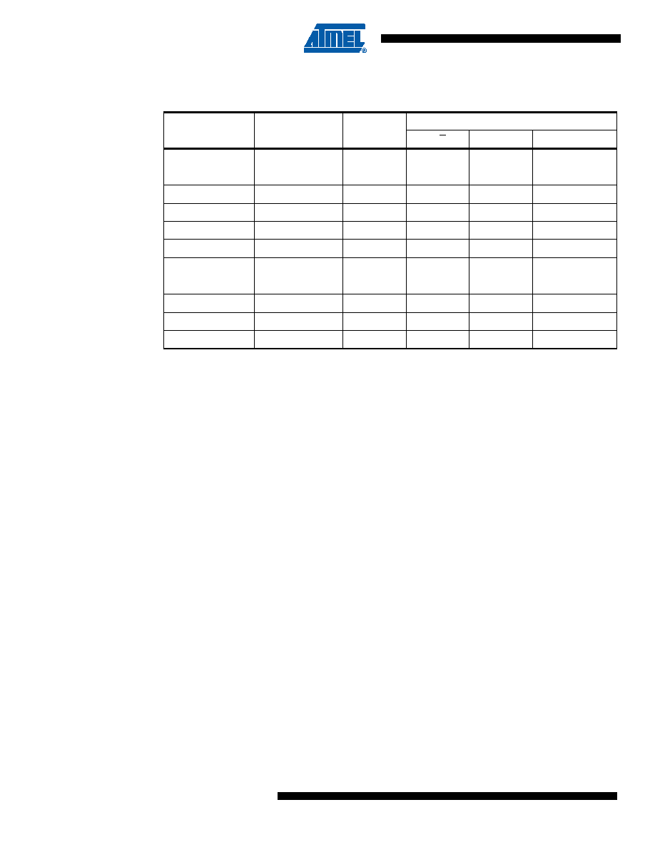
Table 18-2 lists commonly used baud rates and how they can be obtained from Timer 1.
18.3
More About Mode 0
Serial data enters and exits through RXD. TXD outputs the shift clock. Eight data bits are trans-
mitted/received, with the LSB first. The baud rate is fixed at 1/2 the oscillator frequency. Figure
18-1 shows a simplified functional diagram of the serial port in Mode 0 and associated timing.
Transmission is initiated by any instruction that uses SBUF as a destination register. The “write
to SBUF” signal also loads a “1” into the ninth position of the transmit shift register and tells the
TX Control block to begin a transmission. The internal timing is such that one full machine cycle
will elapse between “write to SBUF” and activation of SEND.
SEND transfers the output of the shift register to the alternate output function line of P3.0, and
also transfers Shift Clock to the alternate output function line of P3.1. At the falling edge of Shift
Clock the contents of the transmit shift register are shifted one position to the right.
As data bits shift out to the right, “0”s come in from the left. When the MSB of the data byte is at
the output position of the shift register, the “1” that was initially loaded into the ninth position is
just to the left of the MSB, and all positions to the left of that contain “0”s. This condition flags the
TX Control block to do one last shift, then deactivate SEND and set TI.
Reception is initiated by the condition REN = 1 and R1 = 0. At the next clock cycle, the RX Con-
trol unit writes the bits 11111110 to the receive shift register and activates RECEIVE in the next
clock phase.
RECEIVE enables Shift Clock to the alternate output function line of P3.1. At the falling edge of
Shift Clock the contents of the receive shift register are shifted one position to the left. The value
that comes in from the right is the value that was sampled at the P3.0 pin at rising edge of Shift
Clock.
As data bits come in from the right, “1”s shift out to the left. When the “0” that was initially loaded
into the right-most position arrives at the left-most position in the shift register, it flags the RX
Control block to do one last shift and load SBUF. Then RECEIVE is cleared and RI is set.
Table 18-2.
Commonly Used Baud Rates Generated by Timer 1
Baud Rate
f
OSC (MHz)
SMOD1
Timer 1
C/T
Mode
Reload Value
Mode 0: 1 MHz
2
X
Mode 2: 375K
12
0
X
62.5K
12
102
F4H
19.2K
11.059
1
0
2
DCH
9.6K
11.059
0
2
DCH
4.8K
11.059
0
2
B8H
2.4K
11.059
0
2
70H
1.2K
11.059
0
1
FEE0H
137.5
11.986
0
1
F55CH
110
6
0
1
F958H
110
12
0
1
F304H
相关PDF资料 |
PDF描述 |
|---|---|
| PIC24FJ64GA106-I/MR | MCU PIC 64KB FLASH 64QFN |
| PIC18LF2510-I/SP | IC MCU FLASH 16KX16 28-DIP |
| PIC16C57-XTI/P | IC MCU OTP 2KX12 28DIP |
| ATMEGA88V-10PU | IC AVR MCU 8K 10MHZ 1.8V 28DIP |
| DSPIC33FJ64GP206A-I/PT | IC DSPIC MCU/DSP 64K 64-TQFP |
相关代理商/技术参数 |
参数描述 |
|---|---|
| AT89LP4052-16XI | 功能描述:8位微控制器 -MCU Microcontroller RoHS:否 制造商:Silicon Labs 核心:8051 处理器系列:C8051F39x 数据总线宽度:8 bit 最大时钟频率:50 MHz 程序存储器大小:16 KB 数据 RAM 大小:1 KB 片上 ADC:Yes 工作电源电压:1.8 V to 3.6 V 工作温度范围:- 40 C to + 105 C 封装 / 箱体:QFN-20 安装风格:SMD/SMT |
| AT89LP4052-16XU | 功能描述:8位微控制器 -MCU Microcontroller RoHS:否 制造商:Silicon Labs 核心:8051 处理器系列:C8051F39x 数据总线宽度:8 bit 最大时钟频率:50 MHz 程序存储器大小:16 KB 数据 RAM 大小:1 KB 片上 ADC:Yes 工作电源电压:1.8 V to 3.6 V 工作温度范围:- 40 C to + 105 C 封装 / 箱体:QFN-20 安装风格:SMD/SMT |
| AT89LP4052-20PU | 功能描述:8位微控制器 -MCU SINGLE CYCLE 4K FLASH-20MHZ 2.4-5.5V RoHS:否 制造商:Silicon Labs 核心:8051 处理器系列:C8051F39x 数据总线宽度:8 bit 最大时钟频率:50 MHz 程序存储器大小:16 KB 数据 RAM 大小:1 KB 片上 ADC:Yes 工作电源电压:1.8 V to 3.6 V 工作温度范围:- 40 C to + 105 C 封装 / 箱体:QFN-20 安装风格:SMD/SMT |
| AT89LP4052-20SU | 功能描述:8位微控制器 -MCU SINGLE CYCLE 4K FLASH-20MHZ 2.4-5.5V RoHS:否 制造商:Silicon Labs 核心:8051 处理器系列:C8051F39x 数据总线宽度:8 bit 最大时钟频率:50 MHz 程序存储器大小:16 KB 数据 RAM 大小:1 KB 片上 ADC:Yes 工作电源电压:1.8 V to 3.6 V 工作温度范围:- 40 C to + 105 C 封装 / 箱体:QFN-20 安装风格:SMD/SMT |
| AT89LP4052-20XU | 功能描述:8位微控制器 -MCU SINGLE CYC 4K FLASH -20MHZ 2.4-5.5V RoHS:否 制造商:Silicon Labs 核心:8051 处理器系列:C8051F39x 数据总线宽度:8 bit 最大时钟频率:50 MHz 程序存储器大小:16 KB 数据 RAM 大小:1 KB 片上 ADC:Yes 工作电源电压:1.8 V to 3.6 V 工作温度范围:- 40 C to + 105 C 封装 / 箱体:QFN-20 安装风格:SMD/SMT |
发布紧急采购,3分钟左右您将得到回复。