参数资料
| 型号: | AT89LS52-16PC |
| 厂商: | Atmel |
| 文件页数: | 14/39页 |
| 文件大小: | 0K |
| 描述: | IC MCU 8K FLASH LV 16MHZ 40-DIP |
| 标准包装: | 9 |
| 系列: | 89LS |
| 核心处理器: | 8051 |
| 芯体尺寸: | 8-位 |
| 速度: | 16MHz |
| 连通性: | UART/USART |
| 外围设备: | WDT |
| 输入/输出数: | 32 |
| 程序存储器容量: | 8KB(8K x 8) |
| 程序存储器类型: | 闪存 |
| RAM 容量: | 256 x 8 |
| 电压 - 电源 (Vcc/Vdd): | 2.7 V ~ 4 V |
| 振荡器型: | 内部 |
| 工作温度: | 0°C ~ 70°C |
| 封装/外壳: | 40-DIP(0.600",15.24mm) |
| 包装: | 管件 |
第1页第2页第3页第4页第5页第6页第7页第8页第9页第10页第11页第12页第13页当前第14页第15页第16页第17页第18页第19页第20页第21页第22页第23页第24页第25页第26页第27页第28页第29页第30页第31页第32页第33页第34页第35页第36页第37页第38页第39页
21
2601C–MICRO–06/08
AT89LS52
17. Program Memory Lock Bits
The AT89LS52 has three lock bits that can be left unprogrammed (U) or can be programmed (P)
to obtain the additional features listed in Table 17-1.
When lock bit 1 is programmed, the logic level at the EA pin is sampled and latched during reset.
If the device is powered up without a reset, the latch initializes to a random value and holds that
value until reset is activated. The latched value of EA must agree with the current logic level at
that pin in order for the device to function properly.
18. Programming the Flash – Parallel Mode
The AT89LS52 is shipped with the on-chip Flash memory array ready to be programmed. The
programming interface needs a high-voltage (12-volt) program enable signal and is compatible
with conventional third-party Flash or EPROM programmers.
The AT89LS52 code memory array is programmed byte-by-byte.
Programming Algorithm: Before programming the AT89LS52, the address, data, and control
signals should be set up according to the Flash programming mode table (Table 20-1) and Fig-
ure 20-1 and Figure 20-2. To program the AT89LS52, take the following steps:
1.
Input the desired memory location on the address lines.
2.
Input the appropriate data byte on the data lines.
3.
Activate the correct combination of control signals.
4.
Raise EA/V
PP to 12V.
5.
Pulse ALE/PROG once to program a byte in the Flash array or the lock bits. The byte-
write cycle is self-timed and typically takes no more than 50 s. Repeat steps 1
through 5, changing the address and data for the entire array or until the end of the
object file is reached.
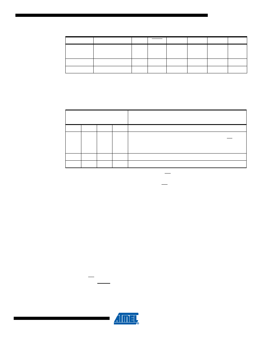
Table 16-1.
Status of External Pins During Idle and Power-down Modes
Mode
Program Memory
ALE
PSEN
PORT0
PORT1
PORT2
PORT3
Idle
Internal
1
Data
Idle
External
1
Float
Data
Address
Data
Power-down
Internal
0
Data
Power-down
External
0
Float
Data
Table 17-1.
Lock Bit Protection Modes
Program Lock Bits
LB1
LB2
LB3
Protection Type
1
U
No program lock features
2P
U
MOVC instructions executed from external program memory are
disabled from fetching code bytes from internal memory, EA is
sampled and latched on reset, and further programming of the
Flash memory is disabled
3
P
U
Same as mode 2, but verify is also disabled
4
P
Same as mode 3, but external execution is also disabled
相关PDF资料 |
PDF描述 |
|---|---|
| AT89LS52-16JI | IC 8051 MCU FLASH 8K 44PLCC |
| AT89LS52-16JC | IC MCU 8K FLASH LV 16MHZ 44-PLCC |
| AT89S52-24PC | IC MCU 8K FLASH 24MHZ 40-DIP |
| AT89S52-24JI | IC MCU 8K FLASH 24MHZ 44-PLCC |
| AT89S52-24JC | IC MCU 8K FLASH 24MHZ 44-PLCC |
相关代理商/技术参数 |
参数描述 |
|---|---|
| AT89LS52-16PI | 功能描述:8位微控制器 -MCU LOW VOLTAGE 8K ISP FLASH - 16MHz RoHS:否 制造商:Silicon Labs 核心:8051 处理器系列:C8051F39x 数据总线宽度:8 bit 最大时钟频率:50 MHz 程序存储器大小:16 KB 数据 RAM 大小:1 KB 片上 ADC:Yes 工作电源电压:1.8 V to 3.6 V 工作温度范围:- 40 C to + 105 C 封装 / 箱体:QFN-20 安装风格:SMD/SMT |
| AT89LS52-16PU | 功能描述:8位微控制器 -MCU LO-VLTG 8K ISP FLASH -16MHZ 2.7-5.5V RoHS:否 制造商:Silicon Labs 核心:8051 处理器系列:C8051F39x 数据总线宽度:8 bit 最大时钟频率:50 MHz 程序存储器大小:16 KB 数据 RAM 大小:1 KB 片上 ADC:Yes 工作电源电压:1.8 V to 3.6 V 工作温度范围:- 40 C to + 105 C 封装 / 箱体:QFN-20 安装风格:SMD/SMT |
| AT89LS52-24AU | 功能描述:8位微控制器 -MCU Microcontroller RoHS:否 制造商:Silicon Labs 核心:8051 处理器系列:C8051F39x 数据总线宽度:8 bit 最大时钟频率:50 MHz 程序存储器大小:16 KB 数据 RAM 大小:1 KB 片上 ADC:Yes 工作电源电压:1.8 V to 3.6 V 工作温度范围:- 40 C to + 105 C 封装 / 箱体:QFN-20 安装风格:SMD/SMT |
| AT89LS52-24JU | 功能描述:8位微控制器 -MCU Microcontroller RoHS:否 制造商:Silicon Labs 核心:8051 处理器系列:C8051F39x 数据总线宽度:8 bit 最大时钟频率:50 MHz 程序存储器大小:16 KB 数据 RAM 大小:1 KB 片上 ADC:Yes 工作电源电压:1.8 V to 3.6 V 工作温度范围:- 40 C to + 105 C 封装 / 箱体:QFN-20 安装风格:SMD/SMT |
| AT89LS52-24PU | 功能描述:8位微控制器 -MCU Microcontroller RoHS:否 制造商:Silicon Labs 核心:8051 处理器系列:C8051F39x 数据总线宽度:8 bit 最大时钟频率:50 MHz 程序存储器大小:16 KB 数据 RAM 大小:1 KB 片上 ADC:Yes 工作电源电压:1.8 V to 3.6 V 工作温度范围:- 40 C to + 105 C 封装 / 箱体:QFN-20 安装风格:SMD/SMT |
发布紧急采购,3分钟左右您将得到回复。