- 您现在的位置:买卖IC网 > PDF目录11723 > AT89S2051-24SU (Atmel)MCU 8051 2K FLASH 24MHZ 20-SOIC PDF资料下载
参数资料
| 型号: | AT89S2051-24SU |
| 厂商: | Atmel |
| 文件页数: | 6/46页 |
| 文件大小: | 0K |
| 描述: | MCU 8051 2K FLASH 24MHZ 20-SOIC |
| 产品培训模块: | MCU Product Line Introduction |
| 标准包装: | 38 |
| 系列: | 89S |
| 核心处理器: | 8051 |
| 芯体尺寸: | 8-位 |
| 速度: | 24MHz |
| 连通性: | UART/USART |
| 外围设备: | 欠压检测/复位,POR,PWM |
| 输入/输出数: | 15 |
| 程序存储器容量: | 2KB(2K x 8) |
| 程序存储器类型: | 闪存 |
| RAM 容量: | 256 x 8 |
| 电压 - 电源 (Vcc/Vdd): | 2.7 V ~ 5.5 V |
| 振荡器型: | 内部 |
| 工作温度: | -40°C ~ 85°C |
| 封装/外壳: | 20-SOIC(0.295",7.50mm 宽) |
| 包装: | 管件 |
第1页第2页第3页第4页第5页当前第6页第7页第8页第9页第10页第11页第12页第13页第14页第15页第16页第17页第18页第19页第20页第21页第22页第23页第24页第25页第26页第27页第28页第29页第30页第31页第32页第33页第34页第35页第36页第37页第38页第39页第40页第41页第42页第43页第44页第45页第46页
14
3390E–MICRO–6/08
AT89S2051/S4051
15. Timer/Counters
The AT89S2051/S4051 have two 16-bit Timer/Counters: Timer 0 and Timer 1. The Timer/Coun-
ters are identical to those in the AT89C2051/C4051. For more detailed information on the
Timer/Counter operation, please click on the document link below:
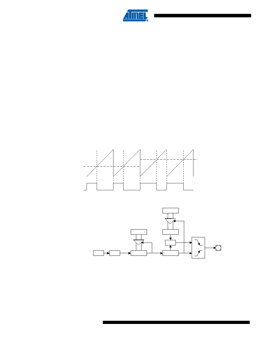
16. Pulse Width Modulation
Timer 0 and Timer 1 may be configured as an 8-bit pulse width modulator by setting the PWMEN
bit in PCON. The generated waveform is output on the Timer 1 input pin, T1. In PWM mode
Timer 0 acts as an 8-bit prescaler to select the PWM timebase. Timer 0 is forced into Mode 2 (8-
bit auto-reload) by PWMEN and the value in TH0 will determine the clock division from 0 (FFh)
to 256 (00h). Timer 1 acts as the 8-bit PWM counter. TL1 counts once on every overflow from
TL0. TH1 stores the 8-bit pulse width value. On the FFh-->00h overflow of TL1, the PWM output
is set high. When the count in TL1 matches the value in TH1, the PWM output is set low. There-
fore, the output pulse width is proportional to the value in TH1. To prevent glitches, writes to TH1
only take effect on the FFh-->00h overflow of TL1. However, a read from TH1 will read the new
value at any time after a write to TH1. See Figure 16-1 for PWM waveform example.
Figure 16-1. Pulse Width Modulation (PWM) Output Waveform
Figure 16-2. Timer 0/1 Pulse Width Modulation Mode
TL0 counts once every machine cycle (1 machine cycle = 12 clocks in X1 mode) and TH0 is the
reload value for when TL0 overflows. Every time TL0 overflows TL1 increments by one, with TL0
overflowing after counting 256 minus TH0 machine cycles.
To calculate the pulse width for the PWM output on pin T1, users should use the following
formula:
TH1 * (256 - TH0) * (1/clock_freq) * 12 = Pulse Width
PWM Output (T1)
Counter Value (TL1)
Compare Value (TH1)
OSC
÷
÷12
TL0
TH0
TH1
TL1
OCR
P3.5
PWM
=?
相关PDF资料 |
PDF描述 |
|---|---|
| VE-B7R-IW-F4 | CONVERTER MOD DC/DC 7.5V 100W |
| GTC02R-22-1S | CONN RCPT 2POS BOX MNT W/SCKT |
| VE-B7P-IX-F3 | CONVERTER MOD DC/DC 13.8V 75W |
| ATTINY44V-10SSU | IC MCU AVR 4K FLASH 10MHZ 14SOIC |
| AT89LS52-16AU | IC MCU 8K FLASH 16MHZ 44-TQFP |
相关代理商/技术参数 |
参数描述 |
|---|---|
| AT89S2051W-16PI | 功能描述:8位微控制器 -MCU Microcontroller RoHS:否 制造商:Silicon Labs 核心:8051 处理器系列:C8051F39x 数据总线宽度:8 bit 最大时钟频率:50 MHz 程序存储器大小:16 KB 数据 RAM 大小:1 KB 片上 ADC:Yes 工作电源电压:1.8 V to 3.6 V 工作温度范围:- 40 C to + 105 C 封装 / 箱体:QFN-20 安装风格:SMD/SMT |
| AT89S2051W-16SI | 功能描述:8位微控制器 -MCU Microcontroller RoHS:否 制造商:Silicon Labs 核心:8051 处理器系列:C8051F39x 数据总线宽度:8 bit 最大时钟频率:50 MHz 程序存储器大小:16 KB 数据 RAM 大小:1 KB 片上 ADC:Yes 工作电源电压:1.8 V to 3.6 V 工作温度范围:- 40 C to + 105 C 封装 / 箱体:QFN-20 安装风格:SMD/SMT |
| AT89S4051-24PU | 功能描述:8位微控制器 -MCU 4K FLASH 24MHZ RoHS:否 制造商:Silicon Labs 核心:8051 处理器系列:C8051F39x 数据总线宽度:8 bit 最大时钟频率:50 MHz 程序存储器大小:16 KB 数据 RAM 大小:1 KB 片上 ADC:Yes 工作电源电压:1.8 V to 3.6 V 工作温度范围:- 40 C to + 105 C 封装 / 箱体:QFN-20 安装风格:SMD/SMT |
| AT89S4051-24SU | 功能描述:8位微控制器 -MCU 4K FLASH 24MHZ RoHS:否 制造商:Silicon Labs 核心:8051 处理器系列:C8051F39x 数据总线宽度:8 bit 最大时钟频率:50 MHz 程序存储器大小:16 KB 数据 RAM 大小:1 KB 片上 ADC:Yes 工作电源电压:1.8 V to 3.6 V 工作温度范围:- 40 C to + 105 C 封装 / 箱体:QFN-20 安装风格:SMD/SMT |
| AT89S4051-24SUR | 功能描述:8051 89S Microcontroller IC 8-Bit 24MHz 4KB (4K x 8) FLASH 20-SOIC 制造商:atmel 系列:89S 包装:管件 零件状态:有效 核心处理器:8051 核心尺寸:8-位 速度:24MHz 连接性:UART/USART 外设:欠压检测/复位,POR,PWM I/O 数:15 程序存储容量:4KB(4K x 8) 程序存储器类型:闪存 EEPROM 容量:- RAM 容量:256 x 8 电压 - 电源(Vcc/Vdd):2.7 V ~ 5.5 V 数据转换器:- 振荡器类型:内部 工作温度:-40°C ~ 85°C(TA) 封装/外壳:20-SOIC(0.295",7.50mm 宽) 供应商器件封装:20-SOIC 标准包装:37 |
发布紧急采购,3分钟左右您将得到回复。