参数资料
| 型号: | AT89S8252-24PI |
| 厂商: | Atmel |
| 文件页数: | 10/41页 |
| 文件大小: | 0K |
| 描述: | MCU W/SPI 8KB FLSH 2K EEP 40-DIP |
| 标准包装: | 9 |
| 系列: | 89S |
| 核心处理器: | 8051 |
| 芯体尺寸: | 8-位 |
| 速度: | 24MHz |
| 连通性: | SPI,UART/USART |
| 外围设备: | POR,WDT |
| 输入/输出数: | 32 |
| 程序存储器容量: | 8KB(8K x 8) |
| 程序存储器类型: | 闪存 |
| EEPROM 大小: | 2K x 8 |
| RAM 容量: | 256 x 8 |
| 电压 - 电源 (Vcc/Vdd): | 4 V ~ 6 V |
| 振荡器型: | 内部 |
| 工作温度: | -40°C ~ 85°C |
| 封装/外壳: | 40-DIP(0.600",15.24mm) |
| 包装: | 管件 |
| 其它名称: | AT89S825224PI |
第1页第2页第3页第4页第5页第6页第7页第8页第9页当前第10页第11页第12页第13页第14页第15页第16页第17页第18页第19页第20页第21页第22页第23页第24页第25页第26页第27页第28页第29页第30页第31页第32页第33页第34页第35页第36页第37页第38页第39页第40页第41页
18
AT89S8252
0401G–MICRO–3/06
UART
The UART in the AT89S8252 operates the same way as the UART in the AT89C51 and
AT89C52. For further information on the UART operation, refer to the Atmel web site
(http://www.atmel.com). From the home page, select “Products”, then “Microcontrollers,
then “8051-Architecture”. Click on “Documentation”, then on “Other Documents”. Open
the document “AT89 Series Hardware Description”.
Serial Peripheral
Interface
The serial peripheral interface (SPI) allows high-speed synchronous data transfer
between the AT89S8252 and peripheral devices or between several AT89S8252
devices. The AT89S8252 SPI features include the following:
Full-Duplex, 3-Wire Synchronous Data Transfer
Master or Slave Operation
1.5 MHz Bit Frequency (max.)
LSB First or MSB First Data Transfer
Four Programmable Bit Rates
End of Transmission Interrupt Flag
Write Collision Flag Protection
Wakeup from Idle Mode (Slave Mode Only)
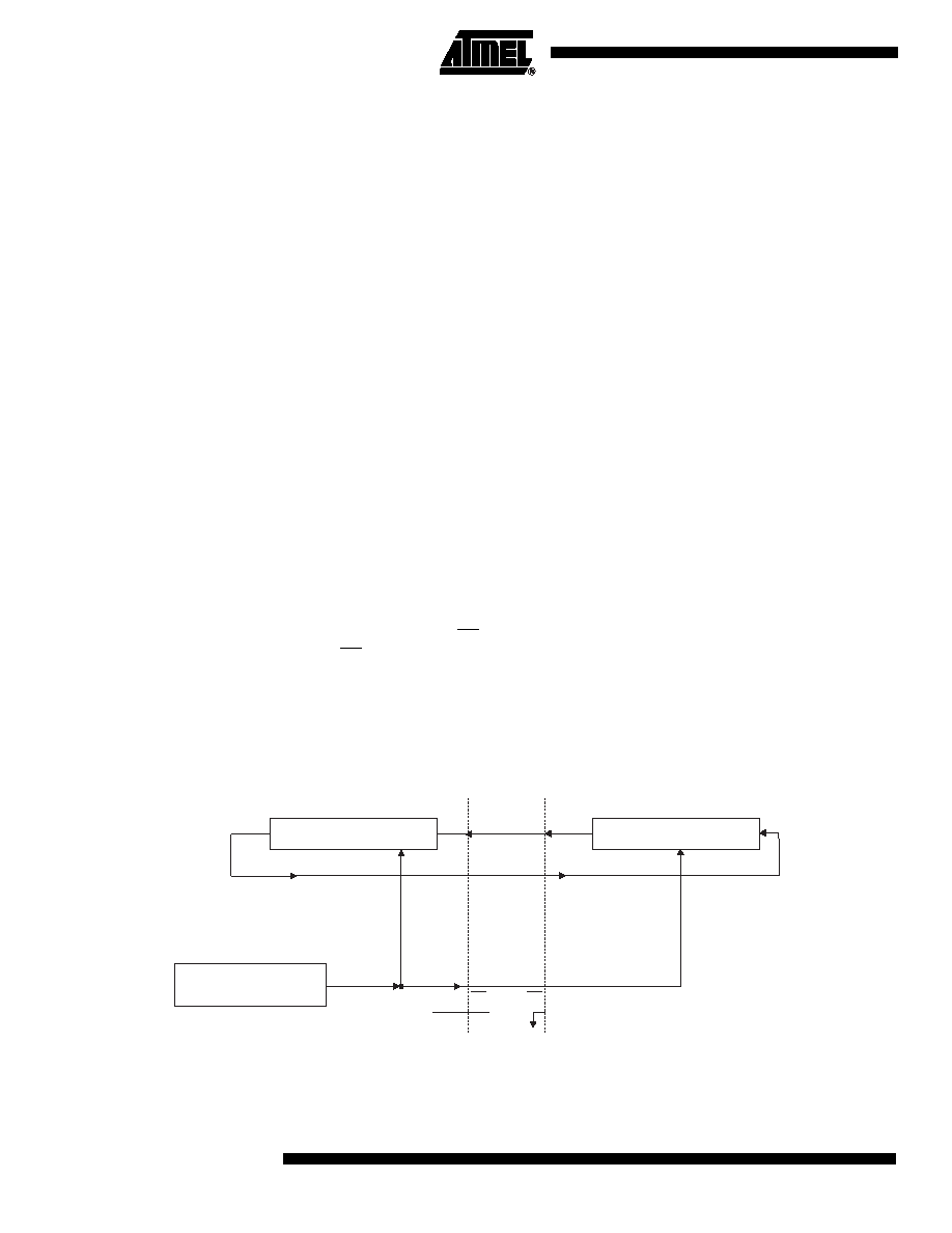
The interconnection between master and slave CPUs with SPI is shown in the following
figure. The SCK pin is the clock output in the master mode but is the clock input in the
slave mode. Writing to the SPI data register of the master CPU starts the SPI clock gen-
erator, and the data written shifts out of the MOSI pin and into the MOSI pin of the slave
CPU. After shifting one byte, the SPI clock generator stops, setting the end of transmis-
sion flag (SPIF). If both the SPI interrupt enable bit (SPIE) and the serial port interrupt
enable bit (ES) are set, an interrupt is requested.
The Slave Select input, SS/P1.4, is set low to select an individual SPI device as a slave.
When SS/P1.4 is set high, the SPI port is deactivated and the MOSI/P1.5 pin can be
used as an input.
There are four combinations of SCK phase and polarity with respect to serial data,
which are determined by control bits CPHA and CPOL. The SPI data transfer formats
Figure 7. SPI Master-slave Interconnection
8-BIT SHIFT REGISTER
MASTER
CLOCK GENERATOR
SPI
MISO
8-BIT SHIFT REGISTER
SLAVE
MISO
MOSI MOSI
SCK
SS
V
CC
MSB
LSB
MSB
LSB
相关PDF资料 |
PDF描述 |
|---|---|
| AT89S8253-24PI | IC 8051 MCU FLASH 12K 40DIP |
| AT90CAN128-15AZ | MCU AVR 128K FLASH 15MHZ 64TQFP |
| AT90CAN128-16MI | IC MCU AVR FLASH 128K 64-QFN |
| AT90CAN64-16AUR | MCU AVR 64K FLASH 16MHZ 64TQFP |
| AT90LS2343-1SI | IC MCU 2K FLASH 1MHZ IND 8-SOIC |
相关代理商/技术参数 |
参数描述 |
|---|---|
| AT89S8252-24QC | 功能描述:8位微控制器 -MCU Microcontroller RoHS:否 制造商:Silicon Labs 核心:8051 处理器系列:C8051F39x 数据总线宽度:8 bit 最大时钟频率:50 MHz 程序存储器大小:16 KB 数据 RAM 大小:1 KB 片上 ADC:Yes 工作电源电压:1.8 V to 3.6 V 工作温度范围:- 40 C to + 105 C 封装 / 箱体:QFN-20 安装风格:SMD/SMT |
| AT89S8252-W | 功能描述:8位微控制器 -MCU Microcontroller RoHS:否 制造商:Silicon Labs 核心:8051 处理器系列:C8051F39x 数据总线宽度:8 bit 最大时钟频率:50 MHz 程序存储器大小:16 KB 数据 RAM 大小:1 KB 片上 ADC:Yes 工作电源电压:1.8 V to 3.6 V 工作温度范围:- 40 C to + 105 C 封装 / 箱体:QFN-20 安装风格:SMD/SMT |
| AT89S8253-24AC | 功能描述:8位微控制器 -MCU Microcontroller RoHS:否 制造商:Silicon Labs 核心:8051 处理器系列:C8051F39x 数据总线宽度:8 bit 最大时钟频率:50 MHz 程序存储器大小:16 KB 数据 RAM 大小:1 KB 片上 ADC:Yes 工作电源电压:1.8 V to 3.6 V 工作温度范围:- 40 C to + 105 C 封装 / 箱体:QFN-20 安装风格:SMD/SMT |
| AT89S8253-24AI | 功能描述:8位微控制器 -MCU UNSAWN WAFER 20 MIL BACKGRIND - 24MHZ RoHS:否 制造商:Silicon Labs 核心:8051 处理器系列:C8051F39x 数据总线宽度:8 bit 最大时钟频率:50 MHz 程序存储器大小:16 KB 数据 RAM 大小:1 KB 片上 ADC:Yes 工作电源电压:1.8 V to 3.6 V 工作温度范围:- 40 C to + 105 C 封装 / 箱体:QFN-20 安装风格:SMD/SMT |
| AT89S8253-24AU | 功能描述:8位微控制器 -MCU 12kB Flash 256B RAM 2.7V-5.5V RoHS:否 制造商:Silicon Labs 核心:8051 处理器系列:C8051F39x 数据总线宽度:8 bit 最大时钟频率:50 MHz 程序存储器大小:16 KB 数据 RAM 大小:1 KB 片上 ADC:Yes 工作电源电压:1.8 V to 3.6 V 工作温度范围:- 40 C to + 105 C 封装 / 箱体:QFN-20 安装风格:SMD/SMT |
发布紧急采购,3分钟左右您将得到回复。