- 您现在的位置:买卖IC网 > PDF目录42902 > ATF-35143-BLK X BAND, Si, N-CHANNEL, RF SMALL SIGNAL, HEMFET PDF资料下载
参数资料
| 型号: | ATF-35143-BLK |
| 元件分类: | 小信号晶体管 |
| 英文描述: | X BAND, Si, N-CHANNEL, RF SMALL SIGNAL, HEMFET |
| 封装: | PLASTIC, SOT-343, 4 PIN |
| 文件页数: | 2/19页 |
| 文件大小: | 126K |
| 代理商: | ATF-35143-BLK |
10
ATF-35143 Typical Noise Parameters
VDS = 3 V, IDS = 10 mA
Freq.
Fmin
Γ
opt
Rn/50
Ga
GHz
dB
Mag.
Ang.
-
dB
0.5
0.12
0.87
4.7
0.21
20.0
0.9
0.16
0.82
13.2
0.19
19.0
1.0
0.17
0.81
15.3
0.19
18.8
1.5
0.22
0.75
25.9
0.17
17.8
1.8
0.26
0.71
32.3
0.16
17.2
2.0
0.28
0.68
36.5
0.16
16.7
2.5
0.33
0.62
47.7
0.14
15.9
3.0
0.39
0.57
59.6
0.13
15.1
4.0
0.49
85.4
0.10
13.7
5.0
0.60
0.43
113.6
0.08
12.5
6.0
0.71
0.38
143.7
0.05
11.4
7.0
0.81
0.36
175.6
0.05
10.4
8.0
0.92
0.34
-151.3
0.07
9.6
9.0
1.03
0.34
-117.3
0.12
8.9
10.0
1.13
0.35
-82.7
0.21
8.4
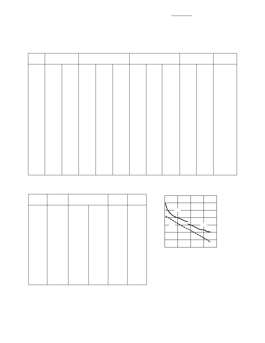
FREQUENCY (GHz)
Figure 22. MSG/MAG and |S21|
2 vs.
Frequency at 3 V, 10 mA.
MSG/MAG
and
S
21
(dB)
020
510
15
MSG
MAG
S21
30
25
20
15
10
5
0
-5
Notes:
1. Fmin values at 2 GHz and higher are based on measurements while the Fmins below 2 GHz have been extrapolated. The Fmin values are
based on a set of 16 noise figure measurements made at 16 different impedances using an ATN NP5 test system. From these measure-
ments a true Fmin is calculated. Refer to the noise parameter application section for more information.
2. S and noise parameters are measured on a microstrip line made on 0.025 inch thick alumina carrier. The input reference plane is at the
end of the gate lead. The output reference plane is at the end of the drain lead. The parameters include the effect of four plated
through via holes connecting source landing pads on top of the test carrier to the microstrip ground plane on the bottom side of the
carrier. Two 0.020 inch diameter via holes are placed within 0.010 inch from each source lead contact point, one via on each side of
that point.
ATF-35143 Typical Scattering Parameters, V
DS = 3 V, IDS = 10 mA
Freq.
S11
S21
S12
S22
MSG/MAG
GHz
Mag.
Ang.
dB
Mag.
Ang.
dB
Mag.
Ang.
Mag.
Ang.
dB
0.50
0.99
-18.76
16.07
6.36
164.73
-32.77
0.023
76.79
0.65
-13.67
24.42
0.75
0.97
-29.12
15.97
6.29
155.93
-29.37
0.034
70.22
0.63
-19.08
22.70
1.00
0.95
-38.28
15.79
6.16
148.37
-27.13
0.044
64.53
0.62
-25.28
21.46
1.50
0.91
-55.52
15.34
5.85
133.87
-24.01
0.063
54.04
0.59
-37.48
19.68
1.75
0.88
-63.78
15.09
5.68
126.95
-22.97
0.071
49.13
0.57
-43.28
19.00
2.00
0.86
-71.79
14.82
5.51
120.22
-22.05
0.079
44.06
0.56
-49.01
18.43
2.50
0.81
-87.55
14.27
5.17
107.29
-20.82
0.091
34.85
0.52
-59.84
17.55
3.00
0.75
-103.15
13.71
4.85
95.00
-19.83
0.102
25.98
0.49
-69.88
16.77
4.00
0.66
-134.65
12.56
4.25
71.95
-18.71
0.116
9.56
0.42
-87.88
15.63
5.00
0.60
-165.16
11.45
3.74
50.50
-18.13
0.124
-5.10
0.35
-105.14
14.79
6.00
0.58
166.12
10.43
3.32
30.44
-17.79
0.129
-19.00
0.29
-122.61
14.11
7.00
0.56
137.25
9.44
2.97
10.91
-17.65
0.131
-32.32
0.23
-141.22
13.55
8.00
0.57
111.11
8.51
2.66
-7.80
-17.59
0.132
-43.61
0.18
-162.07
12.81
9.00
0.60
87.10
7.51
2.38
-26.05
-17.65
0.131
-55.14
0.13
172.01
10.75
10.00
0.64
66.58
6.64
2.15
-43.52
-17.65
0.131
-65.42
0.10
139.11
9.98
11.00
0.68
47.31
5.76
1.94
-61.59
-17.65
0.131
-76.27
0.11
93.44
9.32
12.00
0.71
28.18
4.81
1.74
-79.58
-17.72
0.130
-87.47
0.16
57.88
8.54
13.00
0.74
9.02
3.71
1.53
-96.96
-17.99
0.126
-98.60
0.23
35.32
7.59
14.00
0.77
-4.82
2.61
1.35
-112.95
-18.34
0.121
-107.41
0.29
13.11
6.76
15.00
0.82
-15.65
1.60
1.20
-128.77
-18.56
0.118
-116.63
0.35
-4.62
6.79
16.00
0.82
-28.00
0.51
1.06
-145.23
-18.71
0.116
-126.02
0.42
-19.61
5.79
17.00
0.84
-40.11
-0.55
0.94
-160.01
-18.71
0.116
-136.14
0.49
-29.62
5.54
18.00
0.86
-55.87
-1.68
0.82
-176.05
-19.25
0.109
-146.13
0.55
-41.92
5.05
相关PDF资料 |
PDF描述 |
|---|---|
| ATF-36163-BLKG | KU BAND, GaAs, N-CHANNEL, RF SMALL SIGNAL, HEMFET |
| ATF-36163-TR2 | KU BAND, GaAs, N-CHANNEL, RF SMALL SIGNAL, HEMFET |
| ATF-36163-TR1 | KU BAND, GaAs, N-CHANNEL, RF SMALL SIGNAL, HEMFET |
| ATF-36163-TR2G | KU BAND, GaAs, N-CHANNEL, RF SMALL SIGNAL, HEMFET |
| ATF-36163-TR1G | KU BAND, GaAs, N-CHANNEL, RF SMALL SIGNAL, HEMFET |
相关代理商/技术参数 |
参数描述 |
|---|---|
| ATF-35143-BLKG | 功能描述:射频GaAs晶体管 Transistor GaAs Low Noise RoHS:否 制造商:TriQuint Semiconductor 技术类型:pHEMT 频率:500 MHz to 3 GHz 增益:10 dB 噪声系数: 正向跨导 gFS(最大值/最小值):4 S 漏源电压 VDS: 闸/源击穿电压:- 8 V 漏极连续电流:3 A 最大工作温度:+ 150 C 功率耗散:10 W 安装风格: 封装 / 箱体: |
| ATF-35143-TR1 | 制造商:AGILENT 制造商全称:AGILENT 功能描述:Low Noise Pseudomorphic HEMT in a Surface Mount Plastic Package |
| ATF-35143-TR1G | 功能描述:射频GaAs晶体管 Transistor GaAs Low Noise RoHS:否 制造商:TriQuint Semiconductor 技术类型:pHEMT 频率:500 MHz to 3 GHz 增益:10 dB 噪声系数: 正向跨导 gFS(最大值/最小值):4 S 漏源电压 VDS: 闸/源击穿电压:- 8 V 漏极连续电流:3 A 最大工作温度:+ 150 C 功率耗散:10 W 安装风格: 封装 / 箱体: |
| ATF-35143-TR2 | 制造商:AGILENT 制造商全称:AGILENT 功能描述:Low Noise Pseudomorphic HEMT in a Surface Mount Plastic Package |
| ATF-35143-TR2G | 功能描述:射频GaAs晶体管 Transistor GaAs Low Noise RoHS:否 制造商:TriQuint Semiconductor 技术类型:pHEMT 频率:500 MHz to 3 GHz 增益:10 dB 噪声系数: 正向跨导 gFS(最大值/最小值):4 S 漏源电压 VDS: 闸/源击穿电压:- 8 V 漏极连续电流:3 A 最大工作温度:+ 150 C 功率耗散:10 W 安装风格: 封装 / 箱体: |
发布紧急采购,3分钟左右您将得到回复。