- 您现在的位置:买卖IC网 > PDF目录19655 > ATF1508ASV-15QC100 (Atmel)IC CPLD 128 MACROCELL LV 100PQFP PDF资料下载
参数资料
| 型号: | ATF1508ASV-15QC100 |
| 厂商: | Atmel |
| 文件页数: | 7/28页 |
| 文件大小: | 0K |
| 描述: | IC CPLD 128 MACROCELL LV 100PQFP |
| 标准包装: | 66 |
| 系列: | ATF15xx |
| 可编程类型: | 系统内可编程(最少 10,000 次编程/擦除循环) |
| 最大延迟时间 tpd(1): | 15.0ns |
| 电压电源 - 内部: | 3 V ~ 3.6 V |
| 宏单元数: | 128 |
| 输入/输出数: | 80 |
| 工作温度: | 0°C ~ 70°C |
| 安装类型: | 表面贴装 |
| 封装/外壳: | 100-BQFP |
| 供应商设备封装: | 100-PQFP(14x20) |
| 包装: | 托盘 |
| 其它名称: | ATF1508ASV15QC100 |
第1页第2页第3页第4页第5页第6页当前第7页第8页第9页第10页第11页第12页第13页第14页第15页第16页第17页第18页第19页第20页第21页第22页第23页第24页第25页第26页第27页第28页
15
ATF1508ASV(L)
1408H–PLD–7/05
JTAG-BST Overview
The JTAG-BST (JTAG boundary-scan testing) is controlled by the Test Access Port
(TAP) controller in the ATF1508ASV(L). The boundary-scan technique involves the
inclusion of a shift-register stage (contained in a boundary-scan cell) adjacent to each
component so that signals at component boundaries can be controlled and observed
using scan testing principles. Each input pin and I/O pin has its own Boundary-scan Cell
(BSC) in order to support boundary-scan testing. The ATF1508ASV(L) does not cur-
rently include a Test Reset (TRST) input pin because the TAP controller is automatically
reset at power-up. The six JTAG-BST modes supported include: SAMPLE/PRELOAD,
EXTEST, BYPASS and IDCODE. BST on the ATF1508ASV(L) is implemented using
the Boundary-scan Definition Language (BSDL) described in the JTAG specification
(IEEE Standard 1149.1). Any third-party tool that supports the BSDL format can be used
to perform BST on the ATF1508ASV(L).
The ATF1508ASV(L) also has the option of using four JTAG-standard I/O pins for in-
system programming (ISP). The ATF1508ASV(L) is programmable through the four
JTAG pins using programming-compatible with the IEEE JTAG Standard 1149.1. Pro-
gramming is performed by using 5V TTL-level programming signals from the JTAG ISP
interface. The JTAG feature is a programmable option. If JTAG (BST or ISP) is not
needed, then the four JTAG control pins are available as I/O pins.
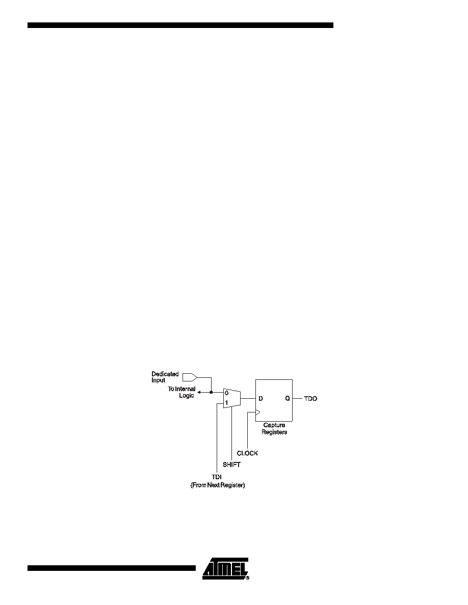
JTAG Boundary-scan
Cell (BSC) Testing
The ATF1508ASV(L) contains up to 96 I/O pins and four input pins, depending on the
device type and package type selected. Each input pin and I/O pin has its own bound-
ary-scan cell (BSC) in order to support boundary-scan testing as described in detail by
IEEE Standard 1149.1. A typical BSC consists of three capture registers or scan regis-
ters and up to two update registers. There are two types of BSCs, one for input or I/O
pin, and one for the macrocells. The BSCs in the device are chained together through
the (BST) capture registers. Input to the capture register chain is fed in from the TDI pin
while the output is directed to the TDO pin. Capture registers are used to capture active
device data signals, to shift data in and out of the device and to load data into the update
registers. Control signals are generated internally by the JTAG TAP controller. The BSC
configuration for the input and I/O pins and macrocells are shown below.
BSC Configuration Pins and Macrocells (Except JTAG TAP Pins)
Note:
The ATF1508ASV(L) has pull-up option on TMS and TDI pins. This feature is selected as a design option.
相关PDF资料 |
PDF描述 |
|---|---|
| ATF1508ASV-15JC84 | IC CPLD 128 MACROCELL LV 84PLCC |
| NMR108C | CONV DC/DC 1W 12VIN 15V SIP SGL |
| ATF1508ASV-15AC100 | IC CPLD 128 MACROCELL LV 100TQFP |
| VE-BW3-CW-B1 | CONVERTER MOD DC/DC 24V 100W |
| GBM06DSEN | CONN EDGECARD 12POS .156 EYELET |
相关代理商/技术参数 |
参数描述 |
|---|---|
| ATF1508ASV-15QC160 | 功能描述:CPLD - 复杂可编程逻辑器件 ASICS RoHS:否 制造商:Lattice 系列: 存储类型:EEPROM 大电池数量:128 最大工作频率:333 MHz 延迟时间:2.7 ns 可编程输入/输出端数量:64 工作电源电压:3.3 V 最大工作温度:+ 90 C 最小工作温度:0 C 封装 / 箱体:TQFP-100 |
| ATF1508ASV-15QI100 | 功能描述:CPLD - 复杂可编程逻辑器件 ASICS RoHS:否 制造商:Lattice 系列: 存储类型:EEPROM 大电池数量:128 最大工作频率:333 MHz 延迟时间:2.7 ns 可编程输入/输出端数量:64 工作电源电压:3.3 V 最大工作温度:+ 90 C 最小工作温度:0 C 封装 / 箱体:TQFP-100 |
| ATF1508ASV-15QI160 | 功能描述:CPLD - 复杂可编程逻辑器件 ASICS RoHS:否 制造商:Lattice 系列: 存储类型:EEPROM 大电池数量:128 最大工作频率:333 MHz 延迟时间:2.7 ns 可编程输入/输出端数量:64 工作电源电压:3.3 V 最大工作温度:+ 90 C 最小工作温度:0 C 封装 / 箱体:TQFP-100 |
| ATF1508ASVL | 制造商:ATMEL 制造商全称:ATMEL Corporation 功能描述:Highperformance EE PLD |
| ATF1508ASVL-20AC100 | 功能描述:CPLD - 复杂可编程逻辑器件 128 MACROCELL w/ISP LO-PWR 3.3V-20NS RoHS:否 制造商:Lattice 系列: 存储类型:EEPROM 大电池数量:128 最大工作频率:333 MHz 延迟时间:2.7 ns 可编程输入/输出端数量:64 工作电源电压:3.3 V 最大工作温度:+ 90 C 最小工作温度:0 C 封装 / 箱体:TQFP-100 |
发布紧急采购,3分钟左右您将得到回复。