- 您现在的位置:买卖IC网 > PDF目录11806 > ATMEGA128A-MUR (Atmel)MCU AVR 128K FLASH 16MHZ 64QFN PDF资料下载
参数资料
| 型号: | ATMEGA128A-MUR |
| 厂商: | Atmel |
| 文件页数: | 155/386页 |
| 文件大小: | 0K |
| 描述: | MCU AVR 128K FLASH 16MHZ 64QFN |
| 产品培训模块: | megaAVR Introduction |
| 标准包装: | 4,000 |
| 系列: | AVR® ATmega |
| 核心处理器: | AVR |
| 芯体尺寸: | 8-位 |
| 速度: | 16MHz |
| 连通性: | EBI/EMI,I²C,SPI,UART/USART |
| 外围设备: | 欠压检测/复位,POR,PWM,WDT |
| 输入/输出数: | 53 |
| 程序存储器容量: | 128KB(64K x 16) |
| 程序存储器类型: | 闪存 |
| EEPROM 大小: | 4K x 8 |
| RAM 容量: | 4K x 8 |
| 电压 - 电源 (Vcc/Vdd): | 2.7 V ~ 5.5 V |
| 数据转换器: | A/D 8x10b |
| 振荡器型: | 内部 |
| 工作温度: | -40°C ~ 85°C |
| 封装/外壳: | 64-VFQFN 裸露焊盘 |
| 包装: | 带卷 (TR) |
| 其它名称: | ATMEGA128A-MUR-ND |
第1页第2页第3页第4页第5页第6页第7页第8页第9页第10页第11页第12页第13页第14页第15页第16页第17页第18页第19页第20页第21页第22页第23页第24页第25页第26页第27页第28页第29页第30页第31页第32页第33页第34页第35页第36页第37页第38页第39页第40页第41页第42页第43页第44页第45页第46页第47页第48页第49页第50页第51页第52页第53页第54页第55页第56页第57页第58页第59页第60页第61页第62页第63页第64页第65页第66页第67页第68页第69页第70页第71页第72页第73页第74页第75页第76页第77页第78页第79页第80页第81页第82页第83页第84页第85页第86页第87页第88页第89页第90页第91页第92页第93页第94页第95页第96页第97页第98页第99页第100页第101页第102页第103页第104页第105页第106页第107页第108页第109页第110页第111页第112页第113页第114页第115页第116页第117页第118页第119页第120页第121页第122页第123页第124页第125页第126页第127页第128页第129页第130页第131页第132页第133页第134页第135页第136页第137页第138页第139页第140页第141页第142页第143页第144页第145页第146页第147页第148页第149页第150页第151页第152页第153页第154页当前第155页第156页第157页第158页第159页第160页第161页第162页第163页第164页第165页第166页第167页第168页第169页第170页第171页第172页第173页第174页第175页第176页第177页第178页第179页第180页第181页第182页第183页第184页第185页第186页第187页第188页第189页第190页第191页第192页第193页第194页第195页第196页第197页第198页第199页第200页第201页第202页第203页第204页第205页第206页第207页第208页第209页第210页第211页第212页第213页第214页第215页第216页第217页第218页第219页第220页第221页第222页第223页第224页第225页第226页第227页第228页第229页第230页第231页第232页第233页第234页第235页第236页第237页第238页第239页第240页第241页第242页第243页第244页第245页第246页第247页第248页第249页第250页第251页第252页第253页第254页第255页第256页第257页第258页第259页第260页第261页第262页第263页第264页第265页第266页第267页第268页第269页第270页第271页第272页第273页第274页第275页第276页第277页第278页第279页第280页第281页第282页第283页第284页第285页第286页第287页第288页第289页第290页第291页第292页第293页第294页第295页第296页第297页第298页第299页第300页第301页第302页第303页第304页第305页第306页第307页第308页第309页第310页第311页第312页第313页第314页第315页第316页第317页第318页第319页第320页第321页第322页第323页第324页第325页第326页第327页第328页第329页第330页第331页第332页第333页第334页第335页第336页第337页第338页第339页第340页第341页第342页第343页第344页第345页第346页第347页第348页第349页第350页第351页第352页第353页第354页第355页第356页第357页第358页第359页第360页第361页第362页第363页第364页第365页第366页第367页第368页第369页第370页第371页第372页第373页第374页第375页第376页第377页第378页第379页第380页第381页第382页第383页第384页第385页第386页
238
8151H–AVR–02/11
ATmega128A
23.5.1
Differential Gain Channels
When using differential gain channels, certain aspects of the conversion need to be taken into
consideration.
Differential conversions are synchronized to the internal clock CK
ADC2 equal to half the ADC
clock. This synchronization is done automatically by the ADC interface in such a way that the
sample-and-hold occurs at a specific edge of CK
ADC2. A conversion initiated by the user (that is,
all single conversions, and the first free running conversion) when CK
ADC2 is low will take the
same amount of time as a single ended conversion (13 ADC clock cycles from the next pres-
caled clock cycle). A conversion initiated by the user when CK
ADC2 is high will take 14 ADC clock
cycles due to the synchronization mechanism. In free running mode, a new conversion is initi-
ated immediately after the previous conversion completes, and since CK
ADC2 is high at this time,
all automatically started (that is, all but the first) free running conversions will take 14 ADC clock
cycles.
The gain stage is optimized for a bandwidth of 4kHz at all gain settings. Higher frequencies may
be subjected to non-linear amplification. An external low-pass filter should be used if the input
signal contains higher frequency components than the gain stage bandwidth. Note that the ADC
clock frequency is independent of the gain stage bandwidth limitation. For example the ADC
clock period may be 6 s, allowing a channel to be sampled at 12 kSPS, regardless of the band-
width of this channel.
23.6
Changing Channel or Reference Selection
The MUXn and REFS1:0 bits in the ADMUX Register are single buffered through a temporary
register to which the CPU has random access. This ensures that the channels and reference
selection only takes place at a safe point during the conversion. The channel and reference
selection is continuously updated until a conversion is started. Once the conversion starts, the
channel and reference selection is locked to ensure a sufficient sampling time for the ADC. Con-
tinuous updating resumes in the last ADC clock cycle before the conversion completes (ADIF in
ADCSRA is set). Note that the conversion starts on the following rising ADC clock edge after
ADSC is written. The user is thus advised not to write new channel or reference selection values
to ADMUX until one ADC clock cycle after ADSC is written.
Special care should be taken when changing differential channels. Once a differential channel
has been selected, the gain stage may take as much as 125 s to stabilize to the new value.
Thus conversions should not be started within the first 125 s after selecting a new differential
channel. Alternatively, conversion results obtained within this period should be discarded.
The same settling time should be observed for the first differential conversion after changing
ADC reference (by changing the REFS1:0 bits in ADMUX).
If the JTAG Interface is enabled, the function of ADC channels on PORTF7:4 is overridden.
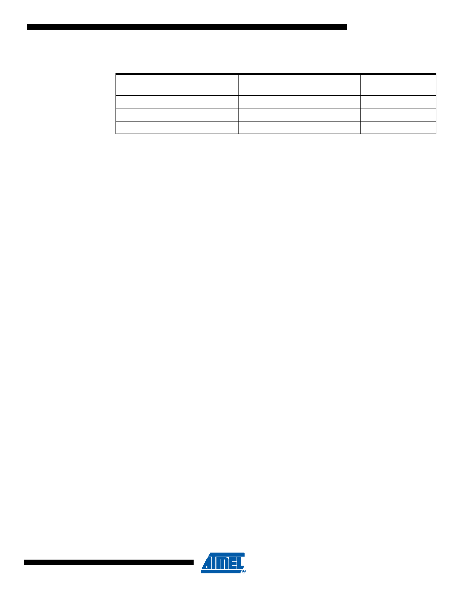
Table 23-1.
ADC Conversion Time
Condition
Sample & Hold (Cycles from Start
of Conversion)
Conversion Time
(Cycles)
First conversion
13.5
25
Normal conversions, single ended
1.5
13
Normal conversions, differential
1.5/2.5
13/14
相关PDF资料 |
PDF描述 |
|---|---|
| LTC4305CGN#PBF | IC BUFFER BUS 2WR ADDRESS 16SSOP |
| LTC1755EGN#PBF | IC SMART CARD INTERFACE 24SSOP |
| AT32UC3C264C-A2UR | IC MCU AVR32 64K FLASH 64TQFP |
| LTC1756EGN#PBF | IC SMART CARD INTERFACE 16SSOP |
| AT89C51IC2-RLRUL | IC 8051 MCU 32K FLASH 44-VQFP |
相关代理商/技术参数 |
参数描述 |
|---|---|
| ATMEGA128CAN11 | 制造商:ATMEL 制造商全称:ATMEL Corporation 功能描述:DEBUG AVR APPLICATIONS USING JTAG OR DEBUGWIRE INTERFACE |
| ATMEGA128L | 制造商:ATMEL 制造商全称:ATMEL Corporation 功能描述:8-bit Microcontroller with 128K Bytes In-System Programmable Flash |
| ATMEGA128L8AC | 制造商:Atmel Corporation 功能描述: |
| ATMEGA128L-8AC | 功能描述:8位微控制器 -MCU AVR 1K FLSH 64B EE 64B SRAM ADC 8MHZ RoHS:否 制造商:Silicon Labs 核心:8051 处理器系列:C8051F39x 数据总线宽度:8 bit 最大时钟频率:50 MHz 程序存储器大小:16 KB 数据 RAM 大小:1 KB 片上 ADC:Yes 工作电源电压:1.8 V to 3.6 V 工作温度范围:- 40 C to + 105 C 封装 / 箱体:QFN-20 安装风格:SMD/SMT |
| ATMEGA128L-8AI | 功能描述:8位微控制器 -MCU AVR 1K FLSH 64B EE 64B SRAM ADC 8MHZ RoHS:否 制造商:Silicon Labs 核心:8051 处理器系列:C8051F39x 数据总线宽度:8 bit 最大时钟频率:50 MHz 程序存储器大小:16 KB 数据 RAM 大小:1 KB 片上 ADC:Yes 工作电源电压:1.8 V to 3.6 V 工作温度范围:- 40 C to + 105 C 封装 / 箱体:QFN-20 安装风格:SMD/SMT |
发布紧急采购,3分钟左右您将得到回复。