- 您现在的位置:买卖IC网 > PDF目录12052 > ATMEGA164A-MCH (Atmel)IC MCU AVR 16K 20MHZ 44QFN PDF资料下载
参数资料
| 型号: | ATMEGA164A-MCH |
| 厂商: | Atmel |
| 文件页数: | 54/160页 |
| 文件大小: | 0K |
| 描述: | IC MCU AVR 16K 20MHZ 44QFN |
| 产品培训模块: | MCU Product Line Introduction megaAVR Introduction |
| 标准包装: | 490 |
| 系列: | AVR® ATmega |
| 核心处理器: | AVR |
| 芯体尺寸: | 8-位 |
| 速度: | 20MHz |
| 连通性: | I²C,SPI,UART/USART |
| 外围设备: | 欠压检测/复位,POR,PWM,WDT |
| 输入/输出数: | 32 |
| 程序存储器容量: | 16KB(8K x 16) |
| 程序存储器类型: | 闪存 |
| EEPROM 大小: | 512 x 8 |
| RAM 容量: | 1K x 8 |
| 电压 - 电源 (Vcc/Vdd): | 1.8 V ~ 5.5 V |
| 数据转换器: | A/D 8x10b |
| 振荡器型: | 内部 |
| 工作温度: | -40°C ~ 85°C |
| 封装/外壳: | 44-VQFN 裸露焊盘 |
| 包装: | 托盘 |
第1页第2页第3页第4页第5页第6页第7页第8页第9页第10页第11页第12页第13页第14页第15页第16页第17页第18页第19页第20页第21页第22页第23页第24页第25页第26页第27页第28页第29页第30页第31页第32页第33页第34页第35页第36页第37页第38页第39页第40页第41页第42页第43页第44页第45页第46页第47页第48页第49页第50页第51页第52页第53页当前第54页第55页第56页第57页第58页第59页第60页第61页第62页第63页第64页第65页第66页第67页第68页第69页第70页第71页第72页第73页第74页第75页第76页第77页第78页第79页第80页第81页第82页第83页第84页第85页第86页第87页第88页第89页第90页第91页第92页第93页第94页第95页第96页第97页第98页第99页第100页第101页第102页第103页第104页第105页第106页第107页第108页第109页第110页第111页第112页第113页第114页第115页第116页第117页第118页第119页第120页第121页第122页第123页第124页第125页第126页第127页第128页第129页第130页第131页第132页第133页第134页第135页第136页第137页第138页第139页第140页第141页第142页第143页第144页第145页第146页第147页第148页第149页第150页第151页第152页第153页第154页第155页第156页第157页第158页第159页第160页
147
8272E–AVR–04/2013
ATmega164A/PA/324A/PA/644A/PA/1284/P
17.5.3
Using the Output Compare Unit
Since writing TCNT2 in any mode of operation will block all compare matches for one timer clock
cycle, there are risks involved when changing TCNT2 when using the Output Compare channel,
independently of whether the Timer/Counter is running or not. If the value written to TCNT2
equals the OCR2x value, the compare match will be missed, resulting in incorrect waveform
generation. Similarly, do not write the TCNT2 value equal to BOTTOM when the counter is
downcounting.
The setup of the OC2x should be performed before setting the Data Direction Register for the
port pin to output. The easiest way of setting the OC2x value is to use the Force Output Com-
pare (FOC2x) strobe bit in Normal mode. The OC2x Register keeps its value even when
changing between Waveform Generation modes.
Be aware that the COM2x1:0 bits are not double buffered together with the compare value.
Changing the COM2x1:0 bits will take effect immediately.
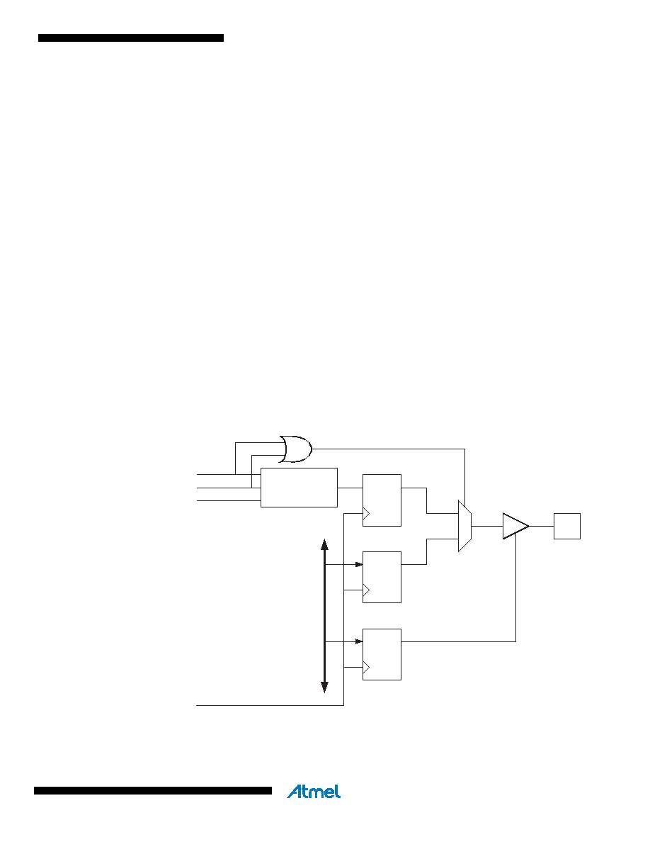
17.6
Compare Match Output unit
The Compare Output mode (COM2x1:0) bits have two functions. The Waveform Generator uses
the COM2x1:0 bits for defining the Output Compare (OC2x) state at the next compare match.
Also, the COM2x1:0 bits control the OC2x pin output source. Figure 17-4 shows a simplified
schematic of the logic affected by the COM2x1:0 bit setting. The I/O Registers, I/O bits, and I/O
pins in the figure are shown in bold. Only the parts of the general I/O Port Control Registers
(DDR and PORT) that are affected by the COM2x1:0 bits are shown. When referring to the
OC2x state, the reference is for the internal OC2x Register, not the OC2x pin.
Figure 17-4. Compare Match Output unit, schematic.
The general I/O port function is overridden by the Output Compare (OC2x) from the Waveform
Generator if either of the COM2x1:0 bits are set. However, the OC2x pin direction (input or out-
put) is still controlled by the Data Direction Register (DDR) for the port pin. The Data Direction
PORT
DDR
DQ
OCnx
Pin
OCnx
DQ
Waveform
Generator
COMnx1
COMnx0
0
1
D
ATA
B
U
S
FOCnx
clk
I/O
相关PDF资料 |
PDF描述 |
|---|---|
| VI-JTZ-IW-F3 | CONVERTER MOD DC/DC 2V 40W |
| ATMEGA168P-20AU | MCU AVR 16K FLASH 20MHZ 32-TQFP |
| VI-J0D-IX-B1 | CONVERTER MOD DC/DC 85V 75W |
| VI-J0B-IX-B1 | CONVERTER MOD DC/DC 95V 75W |
| 859529-4 | 2POS FLANGED RECEPT LGH |
相关代理商/技术参数 |
参数描述 |
|---|---|
| ATMEGA164A-MCHR | 功能描述:8位微控制器 -MCU AVR 16KB FL 512B EE 1KB SRAM-20 MHz RoHS:否 制造商:Silicon Labs 核心:8051 处理器系列:C8051F39x 数据总线宽度:8 bit 最大时钟频率:50 MHz 程序存储器大小:16 KB 数据 RAM 大小:1 KB 片上 ADC:Yes 工作电源电压:1.8 V to 3.6 V 工作温度范围:- 40 C to + 105 C 封装 / 箱体:QFN-20 安装风格:SMD/SMT |
| ATMEGA164A-MU | 功能描述:8位微控制器 -MCU AVR 16KB FL 512B EE 1KB SRAM-20 MHz RoHS:否 制造商:Silicon Labs 核心:8051 处理器系列:C8051F39x 数据总线宽度:8 bit 最大时钟频率:50 MHz 程序存储器大小:16 KB 数据 RAM 大小:1 KB 片上 ADC:Yes 工作电源电压:1.8 V to 3.6 V 工作温度范围:- 40 C to + 105 C 封装 / 箱体:QFN-20 安装风格:SMD/SMT |
| ATMEGA164A-MUR | 功能描述:8位微控制器 -MCU AVR 16KB FL 512B EE 1KB SRAM-20 MHz RoHS:否 制造商:Silicon Labs 核心:8051 处理器系列:C8051F39x 数据总线宽度:8 bit 最大时钟频率:50 MHz 程序存储器大小:16 KB 数据 RAM 大小:1 KB 片上 ADC:Yes 工作电源电压:1.8 V to 3.6 V 工作温度范围:- 40 C to + 105 C 封装 / 箱体:QFN-20 安装风格:SMD/SMT |
| ATMEGA164A-PU | 功能描述:8位微控制器 -MCU AVR 16KB FL 512B EE 1KB SRAM-20 MHz RoHS:否 制造商:Silicon Labs 核心:8051 处理器系列:C8051F39x 数据总线宽度:8 bit 最大时钟频率:50 MHz 程序存储器大小:16 KB 数据 RAM 大小:1 KB 片上 ADC:Yes 工作电源电压:1.8 V to 3.6 V 工作温度范围:- 40 C to + 105 C 封装 / 箱体:QFN-20 安装风格:SMD/SMT |
| ATMEGA164P | 制造商:ATMEL 制造商全称:ATMEL Corporation 功能描述:8-bit Microcontroller with 16/32/64K Bytes In-System Programmable Flash |
发布紧急采购,3分钟左右您将得到回复。