- 您现在的位置:买卖IC网 > PDF目录11213 > ATMEGA324A-CUR (Atmel)IC MCU AVR 32K 20MHZ 49VFBGA PDF资料下载
参数资料
| 型号: | ATMEGA324A-CUR |
| 厂商: | Atmel |
| 文件页数: | 160/160页 |
| 文件大小: | 0K |
| 描述: | IC MCU AVR 32K 20MHZ 49VFBGA |
| 产品培训模块: | MCU Product Line Introduction megaAVR Introduction |
| 标准包装: | 6,000 |
| 系列: | AVR® ATmega |
| 核心处理器: | AVR |
| 芯体尺寸: | 8-位 |
| 速度: | 20MHz |
| 连通性: | I²C,SPI,UART/USART |
| 外围设备: | 欠压检测/复位,POR,PWM,WDT |
| 输入/输出数: | 32 |
| 程序存储器容量: | 32KB(16K x 16) |
| 程序存储器类型: | 闪存 |
| EEPROM 大小: | 1K x 8 |
| RAM 容量: | 2K x 8 |
| 电压 - 电源 (Vcc/Vdd): | 1.8 V ~ 5.5 V |
| 数据转换器: | A/D 8x10b |
| 振荡器型: | 内部 |
| 工作温度: | -40°C ~ 85°C |
| 封装/外壳: | 49-VFBGA |
| 包装: | 带卷 (TR) |
第1页第2页第3页第4页第5页第6页第7页第8页第9页第10页第11页第12页第13页第14页第15页第16页第17页第18页第19页第20页第21页第22页第23页第24页第25页第26页第27页第28页第29页第30页第31页第32页第33页第34页第35页第36页第37页第38页第39页第40页第41页第42页第43页第44页第45页第46页第47页第48页第49页第50页第51页第52页第53页第54页第55页第56页第57页第58页第59页第60页第61页第62页第63页第64页第65页第66页第67页第68页第69页第70页第71页第72页第73页第74页第75页第76页第77页第78页第79页第80页第81页第82页第83页第84页第85页第86页第87页第88页第89页第90页第91页第92页第93页第94页第95页第96页第97页第98页第99页第100页第101页第102页第103页第104页第105页第106页第107页第108页第109页第110页第111页第112页第113页第114页第115页第116页第117页第118页第119页第120页第121页第122页第123页第124页第125页第126页第127页第128页第129页第130页第131页第132页第133页第134页第135页第136页第137页第138页第139页第140页第141页第142页第143页第144页第145页第146页第147页第148页第149页第150页第151页第152页第153页第154页第155页第156页第157页第158页第159页当前第160页
99
8272E–AVR–04/2013
ATmega164A/PA/324A/PA/644A/PA/1284/P
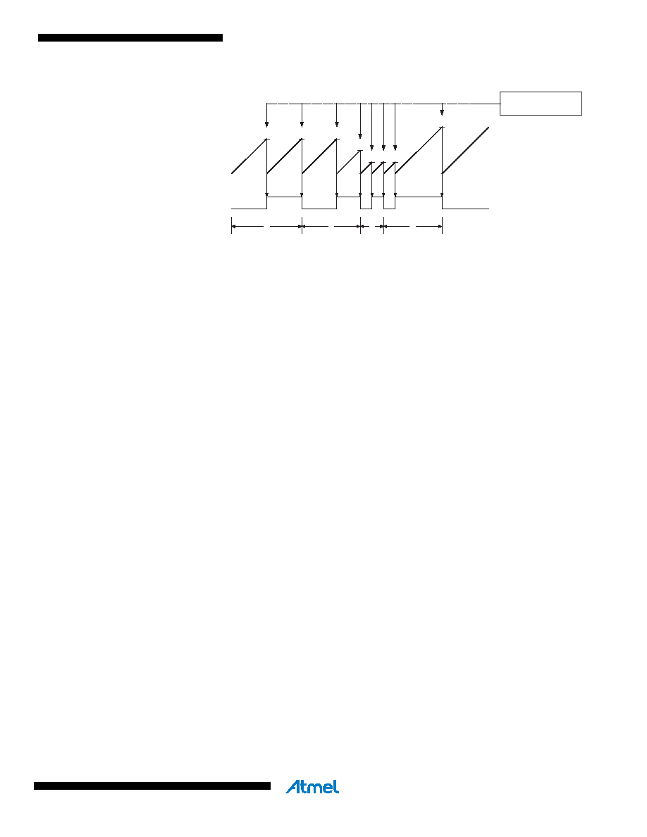
Figure 15-5. CTC mode, timing diagram.
An interrupt can be generated each time the counter value reaches the TOP value by using the
OCF0A Flag. If the interrupt is enabled, the interrupt handler routine can be used for updating
the TOP value. However, changing TOP to a value close to BOTTOM when the counter is run-
ning with none or a low prescaler value must be done with care since the CTC mode does not
have the double buffering feature. If the new value written to OCR0A is lower than the current
value of TCNT0, the counter will miss the Compare Match. The counter will then have to count to
its maximum value (0xFF) and wrap around starting at 0x00 before the Compare Match can
occur.
For generating a waveform output in CTC mode, the OC0A output can be set to toggle its logical
level on each Compare Match by setting the Compare Output mode bits to toggle mode
(COM0A1:0 = 1). The OC0A value will not be visible on the port pin unless the data direction for
the pin is set to output. The waveform generated will have a maximum frequency of f
OC0 =
f
clk_I/O/2 when OCR0A is set to zero (0x00). The waveform frequency is defined by the following
equation:
The N variable represents the prescale factor (1, 8, 64, 256, or 1024).
As for the Normal mode of operation, the TOV0 Flag is set in the same timer clock cycle that the
counter counts from MAX to 0x00.
15.7.3
Fast PWM mode
The fast Pulse Width Modulation or fast PWM mode (WGM02:0 = 3 or 7) provides a high fre-
quency PWM waveform generation option. The fast PWM differs from the other PWM option by
its single-slope operation. The counter counts from BOTTOM to TOP then restarts from BOT-
TOM. TOP is defined as 0xFF when WGM2:0 = 3, and OCR0A when WGM2:0 = 7. In non-
inverting Compare Output mode, the Output Compare (OC0x) is cleared on the Compare Match
between TCNT0 and OCR0x, and set at BOTTOM. In inverting Compare Output mode, the out-
put is set on Compare Match and cleared at BOTTOM. Due to the single-slope operation, the
operating frequency of the fast PWM mode can be twice as high as the phase correct PWM
mode that use dual-slope operation. This high frequency makes the fast PWM mode well suited
for power regulation, rectification, and DAC applications. High frequency allows physically small
sized external components (coils, capacitors), and therefore reduces total system cost.
In fast PWM mode, the counter is incremented until the counter value matches the TOP value.
The counter is then cleared at the following timer clock cycle. The timing diagram for the fast
TCNTn
OCn
(Toggle)
OCnx Interrupt Flag Set
1
4
Period
2
3
(COMnx1:0 = 1)
f
OCnx
f
clk_I/O
2 N
1
OCRnx
+
--------------------------------------------------
=
相关PDF资料 |
PDF描述 |
|---|---|
| VI-B22-IW-F4 | CONVERTER MOD DC/DC 15V 100W |
| VI-B22-IW-F3 | CONVERTER MOD DC/DC 15V 100W |
| VI-B22-IW-F1 | CONVERTER MOD DC/DC 15V 100W |
| AT89LP828-20JU | MCU 8051 8K FLASH SPI 32PLCC |
| VI-B21-IX-F4 | CONVERTER MOD DC/DC 12V 75W |
相关代理商/技术参数 |
参数描述 |
|---|---|
| ATMEGA324A-MCH | 功能描述:8位微控制器 -MCU AVR 32KB FLSH 1KB EE 2KB SRAM-20MHz, IND RoHS:否 制造商:Silicon Labs 核心:8051 处理器系列:C8051F39x 数据总线宽度:8 bit 最大时钟频率:50 MHz 程序存储器大小:16 KB 数据 RAM 大小:1 KB 片上 ADC:Yes 工作电源电压:1.8 V to 3.6 V 工作温度范围:- 40 C to + 105 C 封装 / 箱体:QFN-20 安装风格:SMD/SMT |
| ATMEGA324A-MCHR | 功能描述:8位微控制器 -MCU AVR 32KB FLSH 1KB EE 2KB SRAM-20MHz, IND RoHS:否 制造商:Silicon Labs 核心:8051 处理器系列:C8051F39x 数据总线宽度:8 bit 最大时钟频率:50 MHz 程序存储器大小:16 KB 数据 RAM 大小:1 KB 片上 ADC:Yes 工作电源电压:1.8 V to 3.6 V 工作温度范围:- 40 C to + 105 C 封装 / 箱体:QFN-20 安装风格:SMD/SMT |
| ATMEGA324A-MU | 功能描述:8位微控制器 -MCU AVR 32KB FLSH 1KB EE 2KB SRAM-20MHz, IND RoHS:否 制造商:Silicon Labs 核心:8051 处理器系列:C8051F39x 数据总线宽度:8 bit 最大时钟频率:50 MHz 程序存储器大小:16 KB 数据 RAM 大小:1 KB 片上 ADC:Yes 工作电源电压:1.8 V to 3.6 V 工作温度范围:- 40 C to + 105 C 封装 / 箱体:QFN-20 安装风格:SMD/SMT |
| ATMEGA324A-MUR | 功能描述:8位微控制器 -MCU AVR 32KB FLSH 1KB EE 2KB SRAM-20MHz, IND RoHS:否 制造商:Silicon Labs 核心:8051 处理器系列:C8051F39x 数据总线宽度:8 bit 最大时钟频率:50 MHz 程序存储器大小:16 KB 数据 RAM 大小:1 KB 片上 ADC:Yes 工作电源电压:1.8 V to 3.6 V 工作温度范围:- 40 C to + 105 C 封装 / 箱体:QFN-20 安装风格:SMD/SMT |
| ATMEGA324A-PU | 功能描述:8位微控制器 -MCU AVR 32KB FLSH 1KB EE 2KB SRAM-20MHz, IND RoHS:否 制造商:Silicon Labs 核心:8051 处理器系列:C8051F39x 数据总线宽度:8 bit 最大时钟频率:50 MHz 程序存储器大小:16 KB 数据 RAM 大小:1 KB 片上 ADC:Yes 工作电源电压:1.8 V to 3.6 V 工作温度范围:- 40 C to + 105 C 封装 / 箱体:QFN-20 安装风格:SMD/SMT |
发布紧急采购,3分钟左右您将得到回复。