- 您现在的位置:买卖IC网 > PDF目录11214 > ATMEGA32U2-MUR (Atmel)MCU AVR 32K FLASH 16MHZ 32VQFN PDF资料下载
参数资料
| 型号: | ATMEGA32U2-MUR |
| 厂商: | Atmel |
| 文件页数: | 309/310页 |
| 文件大小: | 0K |
| 描述: | MCU AVR 32K FLASH 16MHZ 32VQFN |
| 产品培训模块: | MCU Product Line Introduction megaAVR Introduction |
| 标准包装: | 5,000 |
| 系列: | AVR® ATmega |
| 核心处理器: | AVR |
| 芯体尺寸: | 8-位 |
| 速度: | 16MHz |
| 连通性: | SPI,UART/USART,USB |
| 外围设备: | 欠压检测/复位,POR,PWM,WDT |
| 输入/输出数: | 22 |
| 程序存储器容量: | 32KB(16K x 16) |
| 程序存储器类型: | 闪存 |
| EEPROM 大小: | 1K x 8 |
| RAM 容量: | 1K x 8 |
| 电压 - 电源 (Vcc/Vdd): | 2.7 V ~ 5.5 V |
| 振荡器型: | 内部 |
| 工作温度: | -40°C ~ 85°C |
| 封装/外壳: | 32-VFQFN 裸露焊盘 |
| 包装: | 带卷 (TR) |
第1页第2页第3页第4页第5页第6页第7页第8页第9页第10页第11页第12页第13页第14页第15页第16页第17页第18页第19页第20页第21页第22页第23页第24页第25页第26页第27页第28页第29页第30页第31页第32页第33页第34页第35页第36页第37页第38页第39页第40页第41页第42页第43页第44页第45页第46页第47页第48页第49页第50页第51页第52页第53页第54页第55页第56页第57页第58页第59页第60页第61页第62页第63页第64页第65页第66页第67页第68页第69页第70页第71页第72页第73页第74页第75页第76页第77页第78页第79页第80页第81页第82页第83页第84页第85页第86页第87页第88页第89页第90页第91页第92页第93页第94页第95页第96页第97页第98页第99页第100页第101页第102页第103页第104页第105页第106页第107页第108页第109页第110页第111页第112页第113页第114页第115页第116页第117页第118页第119页第120页第121页第122页第123页第124页第125页第126页第127页第128页第129页第130页第131页第132页第133页第134页第135页第136页第137页第138页第139页第140页第141页第142页第143页第144页第145页第146页第147页第148页第149页第150页第151页第152页第153页第154页第155页第156页第157页第158页第159页第160页第161页第162页第163页第164页第165页第166页第167页第168页第169页第170页第171页第172页第173页第174页第175页第176页第177页第178页第179页第180页第181页第182页第183页第184页第185页第186页第187页第188页第189页第190页第191页第192页第193页第194页第195页第196页第197页第198页第199页第200页第201页第202页第203页第204页第205页第206页第207页第208页第209页第210页第211页第212页第213页第214页第215页第216页第217页第218页第219页第220页第221页第222页第223页第224页第225页第226页第227页第228页第229页第230页第231页第232页第233页第234页第235页第236页第237页第238页第239页第240页第241页第242页第243页第244页第245页第246页第247页第248页第249页第250页第251页第252页第253页第254页第255页第256页第257页第258页第259页第260页第261页第262页第263页第264页第265页第266页第267页第268页第269页第270页第271页第272页第273页第274页第275页第276页第277页第278页第279页第280页第281页第282页第283页第284页第285页第286页第287页第288页第289页第290页第291页第292页第293页第294页第295页第296页第297页第298页第299页第300页第301页第302页第303页第304页第305页第306页第307页第308页当前第309页第310页
98
7799D–AVR–11/10
ATmega8U2/16U2/32U2
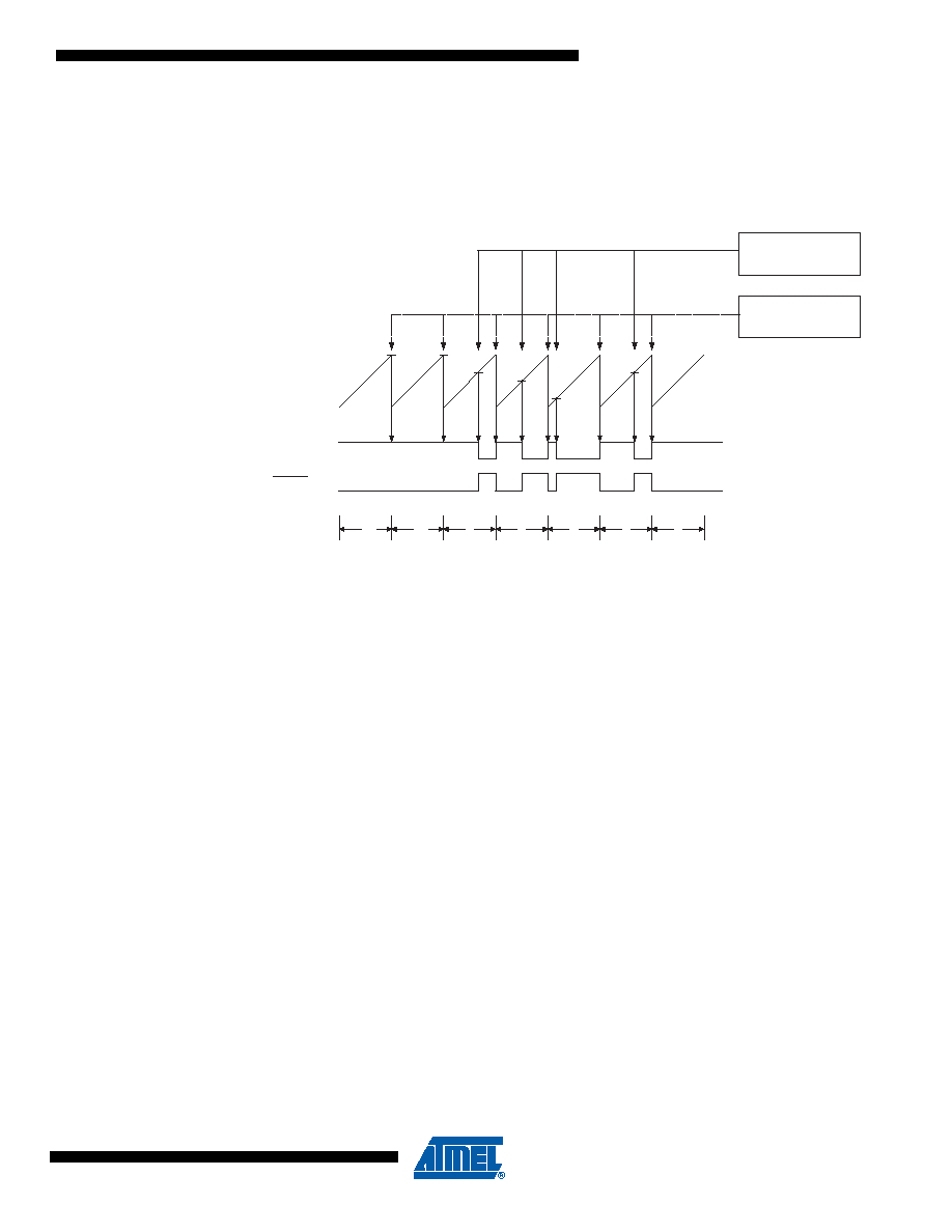
PWM mode is shown in Figure 15-6. The TCNT0 value is in the timing diagram shown as a his-
togram for illustrating the single-slope operation. The diagram includes non-inverted and
inverted PWM outputs. The small horizontal line marks on the TCNT0 slopes represent Com-
pare Matches between OCR0x and TCNT0.
Figure 15-6.
Fast PWM Mode, Timing Diagram
The Timer/Counter Overflow Flag (TOV0) is set each time the counter reaches TOP. If the inter-
rupt is enabled, the interrupt handler routine can be used for updating the compare value.
In fast PWM mode, the compare unit allows generation of PWM waveforms on the OC0x pins.
Setting the COM0x[1:0] bits to two will produce a non-inverted PWM and an inverted PWM out-
put can be generated by setting the COM0x[1:0] to three: Setting the COM0A[1:0] bits to one
allows the OC0A pin to toggle on Compare Matches if the WGM02 bit is set. This option is not
available for the OC0B pin (See Table 15-3 on page 102). The actual OC0x value will only be
visible on the port pin if the data direction for the port pin is set as output. The PWM waveform is
generated by setting (or clearing) the OC0x Register at the Compare Match between OCR0x
and TCNT0, and clearing (or setting) the OC0x Register at the timer clock cycle the counter is
cleared (changes from TOP to BOTTOM).
The PWM frequency for the output can be calculated by the following equation:
The N variable represents the prescale factor (1, 8, 64, 256, or 1024).
The extreme values for the OCR0A Register represents special cases when generating a PWM
waveform output in the fast PWM mode. If the OCR0A is set equal to BOTTOM, the output will
be a narrow spike for each MAX+1 timer clock cycle. Setting the OCR0A equal to MAX will result
in a constantly high or low output (depending on the polarity of the output set by the COM0A1:0
bits.)
A frequency (with 50% duty cycle) waveform output in fast PWM mode can be achieved by set-
ting OC0x to toggle its logical level on each Compare Match (COM0x[1:0] = 1). The waveform
generated will have a maximum frequency of fOC0 = fclk_I/O/2 when OCR0A is set to zero. This
TCNTn
OCRnx Update and
TOVn Interrupt Flag Set
1
Period
2
3
OCnx
(COMnx1:0 = 2)
(COMnx1:0 = 3)
OCRnx Interrupt Flag Set
4
5
6
7
f
OCnxPWM
f clk_I/O
N 256
-------------------
=
相关PDF资料 |
PDF描述 |
|---|---|
| ATMEGA32U2-AUR | MCU AVR 32K FLASH 16MHZ 32TQFP |
| CPC7232KTR | IC ANALOG SWITCH 8CH HV 48-LQFP |
| ATMEGA168V-10AUR | MCU AVR 16KB FLASH 10MHZ 32TQFP |
| ATMEGA168-20MUR | MCU AVR 16KB FLASH 20MHZ 32QFN |
| CPC7232K | IC ANALOG SWITCH 8CH HV 48-LQFP |
相关代理商/技术参数 |
参数描述 |
|---|---|
| ATMEGA32U4 | 制造商:ATMEL 制造商全称:ATMEL Corporation 功能描述:8-bit Microcontroller with 16/32K Bytes of ISP Flash and USB Controller |
| ATMEGA32U4-16AU | 功能描述:8位微控制器 -MCU 32K Flash RoHS:否 制造商:Silicon Labs 核心:8051 处理器系列:C8051F39x 数据总线宽度:8 bit 最大时钟频率:50 MHz 程序存储器大小:16 KB 数据 RAM 大小:1 KB 片上 ADC:Yes 工作电源电压:1.8 V to 3.6 V 工作温度范围:- 40 C to + 105 C 封装 / 箱体:QFN-20 安装风格:SMD/SMT |
| ATMEGA32U4-16MU | 功能描述:8位微控制器 -MCU 32K Flash RoHS:否 制造商:Silicon Labs 核心:8051 处理器系列:C8051F39x 数据总线宽度:8 bit 最大时钟频率:50 MHz 程序存储器大小:16 KB 数据 RAM 大小:1 KB 片上 ADC:Yes 工作电源电压:1.8 V to 3.6 V 工作温度范围:- 40 C to + 105 C 封装 / 箱体:QFN-20 安装风格:SMD/SMT |
| ATMEGA32U4-AU | 功能描述:8位微控制器 -MCU AVR USB 32K FLASH INDUSTRIAL RoHS:否 制造商:Silicon Labs 核心:8051 处理器系列:C8051F39x 数据总线宽度:8 bit 最大时钟频率:50 MHz 程序存储器大小:16 KB 数据 RAM 大小:1 KB 片上 ADC:Yes 工作电源电压:1.8 V to 3.6 V 工作温度范围:- 40 C to + 105 C 封装 / 箱体:QFN-20 安装风格:SMD/SMT |
| ATMEGA32U4-AUR | 功能描述:8位微控制器 -MCU USB 16K FLASH 16 MHz RoHS:否 制造商:Silicon Labs 核心:8051 处理器系列:C8051F39x 数据总线宽度:8 bit 最大时钟频率:50 MHz 程序存储器大小:16 KB 数据 RAM 大小:1 KB 片上 ADC:Yes 工作电源电压:1.8 V to 3.6 V 工作温度范围:- 40 C to + 105 C 封装 / 箱体:QFN-20 安装风格:SMD/SMT |
发布紧急采购,3分钟左右您将得到回复。