- 您现在的位置:买卖IC网 > PDF目录11216 > ATMEGA48PV-10MMUR (Atmel)MCU AVR 4K FLASH 10MHZ 28QFN PDF资料下载
参数资料
| 型号: | ATMEGA48PV-10MMUR |
| 厂商: | Atmel |
| 文件页数: | 224/357页 |
| 文件大小: | 0K |
| 描述: | MCU AVR 4K FLASH 10MHZ 28QFN |
| 产品培训模块: | MCU Product Line Introduction megaAVR Introduction |
| 标准包装: | 6,000 |
| 系列: | AVR® ATmega |
| 核心处理器: | AVR |
| 芯体尺寸: | 8-位 |
| 速度: | 10MHz |
| 连通性: | I²C,SPI,UART/USART |
| 外围设备: | 欠压检测/复位,POR,PWM,WDT |
| 输入/输出数: | 23 |
| 程序存储器容量: | 4KB(2K x 16) |
| 程序存储器类型: | 闪存 |
| EEPROM 大小: | 256 x 8 |
| RAM 容量: | 512 x 8 |
| 电压 - 电源 (Vcc/Vdd): | 1.8 V ~ 5.5 V |
| 数据转换器: | A/D 8x10b |
| 振荡器型: | 内部 |
| 工作温度: | -40°C ~ 85°C |
| 封装/外壳: | 28-VFQFN 裸露焊盘 |
| 包装: | 带卷 (TR) |
第1页第2页第3页第4页第5页第6页第7页第8页第9页第10页第11页第12页第13页第14页第15页第16页第17页第18页第19页第20页第21页第22页第23页第24页第25页第26页第27页第28页第29页第30页第31页第32页第33页第34页第35页第36页第37页第38页第39页第40页第41页第42页第43页第44页第45页第46页第47页第48页第49页第50页第51页第52页第53页第54页第55页第56页第57页第58页第59页第60页第61页第62页第63页第64页第65页第66页第67页第68页第69页第70页第71页第72页第73页第74页第75页第76页第77页第78页第79页第80页第81页第82页第83页第84页第85页第86页第87页第88页第89页第90页第91页第92页第93页第94页第95页第96页第97页第98页第99页第100页第101页第102页第103页第104页第105页第106页第107页第108页第109页第110页第111页第112页第113页第114页第115页第116页第117页第118页第119页第120页第121页第122页第123页第124页第125页第126页第127页第128页第129页第130页第131页第132页第133页第134页第135页第136页第137页第138页第139页第140页第141页第142页第143页第144页第145页第146页第147页第148页第149页第150页第151页第152页第153页第154页第155页第156页第157页第158页第159页第160页第161页第162页第163页第164页第165页第166页第167页第168页第169页第170页第171页第172页第173页第174页第175页第176页第177页第178页第179页第180页第181页第182页第183页第184页第185页第186页第187页第188页第189页第190页第191页第192页第193页第194页第195页第196页第197页第198页第199页第200页第201页第202页第203页第204页第205页第206页第207页第208页第209页第210页第211页第212页第213页第214页第215页第216页第217页第218页第219页第220页第221页第222页第223页当前第224页第225页第226页第227页第228页第229页第230页第231页第232页第233页第234页第235页第236页第237页第238页第239页第240页第241页第242页第243页第244页第245页第246页第247页第248页第249页第250页第251页第252页第253页第254页第255页第256页第257页第258页第259页第260页第261页第262页第263页第264页第265页第266页第267页第268页第269页第270页第271页第272页第273页第274页第275页第276页第277页第278页第279页第280页第281页第282页第283页第284页第285页第286页第287页第288页第289页第290页第291页第292页第293页第294页第295页第296页第297页第298页第299页第300页第301页第302页第303页第304页第305页第306页第307页第308页第309页第310页第311页第312页第313页第314页第315页第316页第317页第318页第319页第320页第321页第322页第323页第324页第325页第326页第327页第328页第329页第330页第331页第332页第333页第334页第335页第336页第337页第338页第339页第340页第341页第342页第343页第344页第345页第346页第347页第348页第349页第350页第351页第352页第353页第354页第355页第356页第357页
2008-2011 Microchip Technology Inc.
DS41364E-page 357
PIC16(L)F1934/6/7
27.11 Operation During Sleep
The LCD module can operate during Sleep. The
selection is controlled by bit SLPEN of the LCDCON
register. Setting the SLPEN bit allows the LCD module
to go to Sleep. Clearing the SLPEN bit allows the
module to continue to operate during Sleep.
If a SLEEP instruction is executed and SLPEN = 1, the
LCD module will cease all functions and go into a very
low-current Consumption mode. The module will stop
operation immediately and drive the minimum LCD
voltage on both segment and common lines.
Figure 27-20 shows this operation.
The LCD module can be configured to operate during
Sleep. The selection is controlled by bit SLPEN of the
LCDCON register. Clearing SLPEN and correctly con-
figuring the LCD module clock will allow the LCD mod-
ule to operate during Sleep. Setting SLPEN and
correctly executing the LCD module shutdown will dis-
able the LCD module during Sleep and save power.
If a SLEEP instruction is executed and SLPEN = 1, the
LCD module will immediately cease all functions, drive
the outputs to Vss and go into a very Low-Current
mode. The SLEEP instruction should only be executed
after the LCD module has been disabled and the cur-
rent cycle completed, thus ensuring that there are no
DC voltages on the glass. To disable the LCD module,
clear the LCDEN bit. The LCD module will complete the
disabling process after the current frame, clear the
LCDA bit and optionally cause an interrupt.
The steps required to properly enter Sleep with the
LCD disabled are:
Clear LCDEN
Wait for LCDA = 0 either by polling or by interrupt
Execute SLEEP
If SLPEN = 0 and SLEEP is executed while the LCD
module clock source is FOSC/4, then the LCD module
will halt with the pin driving the last LCD voltage pat-
tern. Prolonged exposure to a fixed LCD voltage pat-
tern will cause damage to the LCD glass. To prevent
LCD glass damage, either perform the proper LCD
module shutdown prior to Sleep, or change the LCD
module clock to allow the LCD module to continue
operation during Sleep.
If a SLEEP instruction is executed and SLPEN = 0 and
the LCD module clock is either T1OSC or LFINTOSC,
the module will continue to display the current contents
of the LCDDATA registers. While in Sleep, the LCD
data cannot be changed. If the LCDIE bit is set, the
device will wake from Sleep on the next LCD frame
boundary. The LCD module current consumption will
not decrease in this mode; however, the overall device
power consumption will be lower due to the shutdown
of the CPU and other peripherals.
Table 27-8 shows the status of the LCD module during
a Sleep while using each of the three available clock
sources.
If a SLEEP instruction is executed and SLPEN = 0, the
module will continue to display the current contents of
the LCDDATA registers. To allow the module to
continue operation while in Sleep, the clock source
must be either the LFINTOSC or T1OSC external
oscillator. While in Sleep, the LCD data cannot be
changed. The LCD module current consumption will
not decrease in this mode; however, the overall
consumption of the device will be lower due to shut
down of the core and other peripheral functions.
Table 27-8 shows the status of the LCD module during
Sleep while using each of the three available clock
sources:
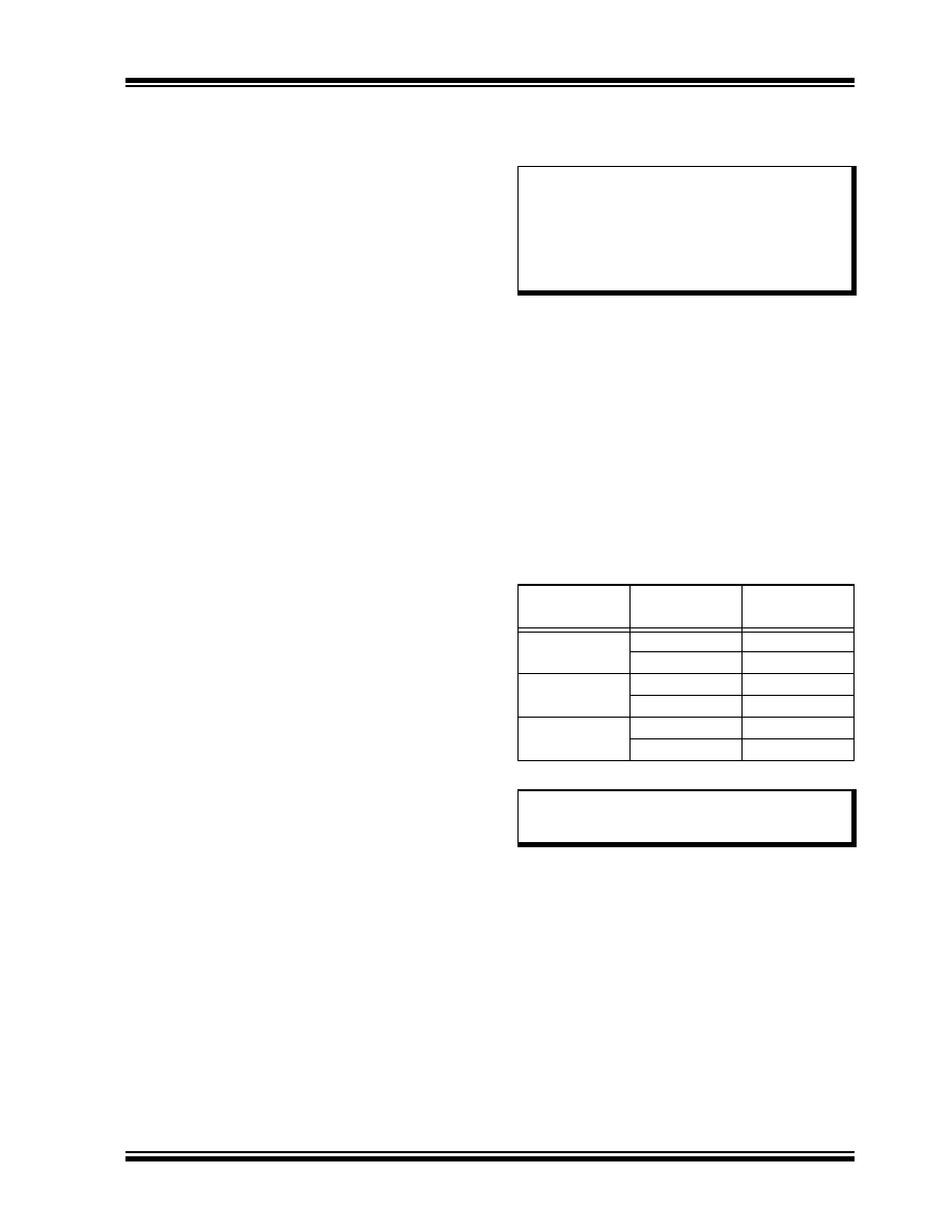
TABLE 27-8:
LCD MODULE STATUS
DURING SLEEP
If LCD interrupts are being generated (Type-B wave-
form with a multiplex mode not static) and LCDIE = 1,
the device will awaken from Sleep on the next frame
boundary.
Note:
When the LCDEN bit is cleared, the LCD
module will be disabled at the completion
of frame. At this time, the port pins will
revert to digital functionality. To minimize
power consumption due to floating digital
inputs, the LCD pins should be driven low
using the PORT and TRIS registers.
Clock Source
SLPEN
Operational
During Sleep
T1OSC
0
Yes
1
No
LFINTOSC
0
Yes
1
No
FOSC/4
0
No
1
No
Note:
The LFINTOSC or external T1OSC
oscillator must be used to operate the
LCD module during Sleep.
相关PDF资料 |
PDF描述 |
|---|---|
| VE-BWT-IX | CONVERTER MOD DC/DC 6.5V 75W |
| ADG726BSUZ-REEL | IC MULTIPLEXER DUAL 16X1 48TQFP |
| VE-B30-IW-F2 | CONVERTER MOD DC/DC 5V 100W |
| ATMEGA48PV-10MUR | MCU AVR 4K FLASH 10MHZ 32QFN |
| ATMEGA48PV-10AUR | MCU AVR 4K FLASH 10MHZ 32TQFP |
相关代理商/技术参数 |
参数描述 |
|---|---|
| ATMEGA48PV-10MU | 功能描述:8位微控制器 -MCU AVR 4K FLASH 256B EE 10MHZ TEMP GRN 1.8V RoHS:否 制造商:Silicon Labs 核心:8051 处理器系列:C8051F39x 数据总线宽度:8 bit 最大时钟频率:50 MHz 程序存储器大小:16 KB 数据 RAM 大小:1 KB 片上 ADC:Yes 工作电源电压:1.8 V to 3.6 V 工作温度范围:- 40 C to + 105 C 封装 / 箱体:QFN-20 安装风格:SMD/SMT |
| ATMEGA48PV-10MUR | 功能描述:8位微控制器 -MCU AVR 4K FLSH 256B EE 512B 5V 10MHz 1.8V RoHS:否 制造商:Silicon Labs 核心:8051 处理器系列:C8051F39x 数据总线宽度:8 bit 最大时钟频率:50 MHz 程序存储器大小:16 KB 数据 RAM 大小:1 KB 片上 ADC:Yes 工作电源电压:1.8 V to 3.6 V 工作温度范围:- 40 C to + 105 C 封装 / 箱体:QFN-20 安装风格:SMD/SMT |
| ATMEGA48PV10PU | 制造商:ATMEL 功能描述:Pb Free |
| ATMEGA48PV-10PU | 功能描述:8位微控制器 -MCU AVR 4K FLASH 256B EE 10MHZ TEMP GRN 1.8V RoHS:否 制造商:Silicon Labs 核心:8051 处理器系列:C8051F39x 数据总线宽度:8 bit 最大时钟频率:50 MHz 程序存储器大小:16 KB 数据 RAM 大小:1 KB 片上 ADC:Yes 工作电源电压:1.8 V to 3.6 V 工作温度范围:- 40 C to + 105 C 封装 / 箱体:QFN-20 安装风格:SMD/SMT |
| ATmega48V-10AI | 功能描述:8位微控制器 -MCU AVR 4K FLASH 256B EE 512B SRAM ADC RoHS:否 制造商:Silicon Labs 核心:8051 处理器系列:C8051F39x 数据总线宽度:8 bit 最大时钟频率:50 MHz 程序存储器大小:16 KB 数据 RAM 大小:1 KB 片上 ADC:Yes 工作电源电压:1.8 V to 3.6 V 工作温度范围:- 40 C to + 105 C 封装 / 箱体:QFN-20 安装风格:SMD/SMT |
发布紧急采购,3分钟左右您将得到回复。