- 您现在的位置:买卖IC网 > PDF目录11216 > ATTINY24V-10SSUR (Atmel)MCU AVR 2KB FLASH 10MHZ 14SOIC PDF资料下载
参数资料
| 型号: | ATTINY24V-10SSUR |
| 厂商: | Atmel |
| 文件页数: | 18/238页 |
| 文件大小: | 0K |
| 描述: | MCU AVR 2KB FLASH 10MHZ 14SOIC |
| 产品培训模块: | tinyAVR Introduction |
| 标准包装: | 3,000 |
| 系列: | AVR® ATtiny |
| 核心处理器: | AVR |
| 芯体尺寸: | 8-位 |
| 速度: | 10MHz |
| 连通性: | USI |
| 外围设备: | 欠压检测/复位,POR,PWM,温度传感器,WDT |
| 输入/输出数: | 12 |
| 程序存储器容量: | 2KB(1K x 16) |
| 程序存储器类型: | 闪存 |
| EEPROM 大小: | 128 x 8 |
| RAM 容量: | 128 x 8 |
| 电压 - 电源 (Vcc/Vdd): | 1.8 V ~ 5.5 V |
| 数据转换器: | A/D 8x10b |
| 振荡器型: | 内部 |
| 工作温度: | -40°C ~ 85°C |
| 封装/外壳: | 14-SOIC(0.154",3.90mm 宽) |
| 包装: | 带卷 (TR) |
| 配用: | ATSTK600-RC46-ND - STK600 ROUTING CARD AVR |
第1页第2页第3页第4页第5页第6页第7页第8页第9页第10页第11页第12页第13页第14页第15页第16页第17页当前第18页第19页第20页第21页第22页第23页第24页第25页第26页第27页第28页第29页第30页第31页第32页第33页第34页第35页第36页第37页第38页第39页第40页第41页第42页第43页第44页第45页第46页第47页第48页第49页第50页第51页第52页第53页第54页第55页第56页第57页第58页第59页第60页第61页第62页第63页第64页第65页第66页第67页第68页第69页第70页第71页第72页第73页第74页第75页第76页第77页第78页第79页第80页第81页第82页第83页第84页第85页第86页第87页第88页第89页第90页第91页第92页第93页第94页第95页第96页第97页第98页第99页第100页第101页第102页第103页第104页第105页第106页第107页第108页第109页第110页第111页第112页第113页第114页第115页第116页第117页第118页第119页第120页第121页第122页第123页第124页第125页第126页第127页第128页第129页第130页第131页第132页第133页第134页第135页第136页第137页第138页第139页第140页第141页第142页第143页第144页第145页第146页第147页第148页第149页第150页第151页第152页第153页第154页第155页第156页第157页第158页第159页第160页第161页第162页第163页第164页第165页第166页第167页第168页第169页第170页第171页第172页第173页第174页第175页第176页第177页第178页第179页第180页第181页第182页第183页第184页第185页第186页第187页第188页第189页第190页第191页第192页第193页第194页第195页第196页第197页第198页第199页第200页第201页第202页第203页第204页第205页第206页第207页第208页第209页第210页第211页第212页第213页第214页第215页第216页第217页第218页第219页第220页第221页第222页第223页第224页第225页第226页第227页第228页第229页第230页第231页第232页第233页第234页第235页第236页第237页第238页
PIC18CXX2
DS39026C-page 112
2001 Microchip Technology Inc.
13.5
PWM Mode
In Pulse Width Modulation (PWM) mode, the CCP1 pin
produces up to a 10-bit resolution PWM output. Since
the CCP1 pin is multiplexed with the PORTC data latch,
the TRISC<2> bit must be cleared to make the CCP1
pin an output.
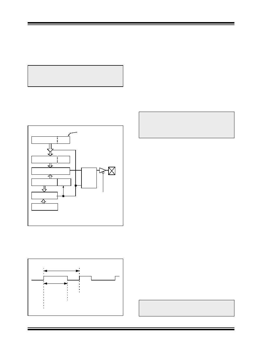
Figure 13-3 shows a simplified block diagram of the
CCP module in PWM mode.
For a step-by-step procedure on how to set up the CCP
module for PWM operation, see Section 13.5.3.
FIGURE 13-3:
SIMPLIFIED PWM BLOCK
DIAGRAM
A PWM output (Figure 13-4) has a time-base (period)
and a time that the output stays high (duty cycle). The
frequency of the PWM is the inverse of the period
(1/period).
FIGURE 13-4:
PWM OUTPUT
13.5.1
PWM PERIOD
The PWM period is specified by writing to the PR2 reg-
ister. The PWM period can be calculated using the fol-
lowing formula:
PWM period = (PR2) + 1] 4 TOSC
(TMR2 prescale value)
PWM frequency is defined as 1 / [PWM period].
When TMR2 is equal to PR2, the following three events
occur on the next increment cycle:
TMR2 is cleared
The CCP1 pin is set (exception: if PWM duty
cycle = 0%, the CCP1 pin will not be set)
The PWM duty cycle is latched from CCPR1L into
CCPR1H
13.5.2
PWM DUTY CYCLE
The PWM duty cycle is specified by writing to the
CCPR1L register and to the CCP1CON<5:4> bits. Up
to 10-bit resolution is available. The CCPR1L contains
the eight MSbs and the CCP1CON<5:4> contains the
two LSbs. This 10-bit value is represented by
CCPR1L:CCP1CON<5:4>. The following equation is
used to calculate the PWM duty cycle in time:
PWM duty cycle
= (CCPR1L:CCP1CON<5:4>)
TOSC (TMR2 prescale value)
CCPR1L and CCP1CON<5:4> can be written to at any
time, but the duty cycle value is not latched into
CCPR1H until after a match between PR2 and TMR2
occurs (i.e., the period is complete). In PWM mode,
CCPR1H is a read only register.
The CCPR1H register and a 2-bit internal latch are
used to double buffer the PWM duty cycle. This double
buffering is essential for glitchless PWM operation.
When the CCPR1H and 2-bit latch match TMR2 con-
catenated with an internal 2-bit Q clock or 2 bits of the
TMR2 prescaler, the CCP1 pin is cleared.
The maximum PWM resolution (bits) for a given PWM
frequency is given by the equation:
Note:
Clearing the CCP1CON register will force
the CCP1 PWM output latch to the default
low level. This is not the PORTC I/O data
latch.
CCPR1L
CCPR1H (Slave)
Comparator
TMR2
Comparator
PR2
(Note 1)
R
Q
S
Duty Cycle Registers
CCP1CON<5:4>
Clear Timer,
CCP1 pin and
latch D.C.
TRISC<2>
RC2/CCP1
Note:
8-bit timer is concatenated with 2-bit internal Q clock or
2 bits of the prescaler to create 10-bit time-base.
Period
Duty Cycle
TMR2 = PR2
TMR2 = Duty Cycle
TMR2 = PR2
Note:
The Timer2 postscaler (see Section 11.0)
is not used in the determination of the
PWM frequency. The postscaler could be
used to have a servo update rate at a dif-
ferent frequency than the PWM output.
Note:
If the PWM duty cycle value is longer than
the PWM period, the CCP1 pin will not be
cleared.
FOSC
FPWM
---------------
log
2
()
log
-----------------------------bits
=
PWM Resolution (max)
相关PDF资料 |
PDF描述 |
|---|---|
| AT90USB82-16MUR | MCU AVR USB 8K FLASH 32-QFN |
| ADG201HSKR-REEL | IC SWITCH QUAD SPST 16SOIC |
| ADG1406BRUZ-REEL7 | IC MULTIPLEXER 8X1 28TSSOP |
| ADG201HSJPZ | IC SWITCH QUAD SPST 20PLCC |
| ADG333ABR | IC SWITCH QUAD SPDT 20SOIC |
相关代理商/技术参数 |
参数描述 |
|---|---|
| ATTINY24V-15MT | 制造商:ATMEL 制造商全称:ATMEL Corporation 功能描述:8-bit Microcontroller with 2/4/8K Bytes In-System Programmable Flash |
| ATTINY24V-15SST | 制造商:ATMEL 制造商全称:ATMEL Corporation 功能描述:8-bit Microcontroller with 2/4/8K Bytes In-System Programmable Flash |
| ATTINY24V-W-11 | 功能描述:8位微控制器 -MCU Microcontroller RoHS:否 制造商:Silicon Labs 核心:8051 处理器系列:C8051F39x 数据总线宽度:8 bit 最大时钟频率:50 MHz 程序存储器大小:16 KB 数据 RAM 大小:1 KB 片上 ADC:Yes 工作电源电压:1.8 V to 3.6 V 工作温度范围:- 40 C to + 105 C 封装 / 箱体:QFN-20 安装风格:SMD/SMT |
| ATTINY25 | 制造商:ATMEL 制造商全称:ATMEL Corporation 功能描述:8-bit Microcontroller with 2/4/8K Bytes In-System Programmable Flash |
| ATTINY25/V | 制造商:ATMEL 制造商全称:ATMEL Corporation 功能描述:8-bit Microcontroller with 2/4/8K Bytes In-System Programmable Flash |
发布紧急采购,3分钟左右您将得到回复。