参数资料
| 型号: | ATTINY261A-MUR |
| 厂商: | Atmel |
| 文件页数: | 23/296页 |
| 文件大小: | 0K |
| 描述: | MCU AVR 2KB FLASH 20MHZ 32QFN |
| 产品培训模块: | tinyAVR Introduction |
| 标准包装: | 6,000 |
| 系列: | AVR® ATtiny |
| 核心处理器: | AVR |
| 芯体尺寸: | 8-位 |
| 速度: | 20MHz |
| 连通性: | USI |
| 外围设备: | 欠压检测/复位,POR,PWM,温度传感器,WDT |
| 输入/输出数: | 16 |
| 程序存储器容量: | 2KB(1K x 16) |
| 程序存储器类型: | 闪存 |
| EEPROM 大小: | 128 x 8 |
| RAM 容量: | 128 x 8 |
| 电压 - 电源 (Vcc/Vdd): | 1.8 V ~ 5.5 V |
| 数据转换器: | A/D 11x10b |
| 振荡器型: | 内部 |
| 工作温度: | -40°C ~ 85°C |
| 封装/外壳: | 32-VFQFN 裸露焊盘 |
| 包装: | 带卷 (TR) |
| 其它名称: | ATTINY261A-MUR-ND ATTINY261A-MURTR |
第1页第2页第3页第4页第5页第6页第7页第8页第9页第10页第11页第12页第13页第14页第15页第16页第17页第18页第19页第20页第21页第22页当前第23页第24页第25页第26页第27页第28页第29页第30页第31页第32页第33页第34页第35页第36页第37页第38页第39页第40页第41页第42页第43页第44页第45页第46页第47页第48页第49页第50页第51页第52页第53页第54页第55页第56页第57页第58页第59页第60页第61页第62页第63页第64页第65页第66页第67页第68页第69页第70页第71页第72页第73页第74页第75页第76页第77页第78页第79页第80页第81页第82页第83页第84页第85页第86页第87页第88页第89页第90页第91页第92页第93页第94页第95页第96页第97页第98页第99页第100页第101页第102页第103页第104页第105页第106页第107页第108页第109页第110页第111页第112页第113页第114页第115页第116页第117页第118页第119页第120页第121页第122页第123页第124页第125页第126页第127页第128页第129页第130页第131页第132页第133页第134页第135页第136页第137页第138页第139页第140页第141页第142页第143页第144页第145页第146页第147页第148页第149页第150页第151页第152页第153页第154页第155页第156页第157页第158页第159页第160页第161页第162页第163页第164页第165页第166页第167页第168页第169页第170页第171页第172页第173页第174页第175页第176页第177页第178页第179页第180页第181页第182页第183页第184页第185页第186页第187页第188页第189页第190页第191页第192页第193页第194页第195页第196页第197页第198页第199页第200页第201页第202页第203页第204页第205页第206页第207页第208页第209页第210页第211页第212页第213页第214页第215页第216页第217页第218页第219页第220页第221页第222页第223页第224页第225页第226页第227页第228页第229页第230页第231页第232页第233页第234页第235页第236页第237页第238页第239页第240页第241页第242页第243页第244页第245页第246页第247页第248页第249页第250页第251页第252页第253页第254页第255页第256页第257页第258页第259页第260页第261页第262页第263页第264页第265页第266页第267页第268页第269页第270页第271页第272页第273页第274页第275页第276页第277页第278页第279页第280页第281页第282页第283页第284页第285页第286页第287页第288页第289页第290页第291页第292页第293页第294页第295页第296页
119
8197C–AVR–05/11
ATtiny261A/461A/861A
the Output Compare Override Enable Bit is cleared. Table 12-22 shows the Output Compare
Override Enable Bits and their corresponding Output Compare pins.
12.12.6
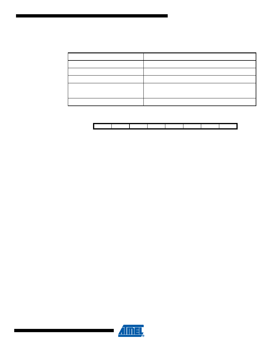
PLLCSR – PLL Control and Status Register
Bit 7 – LSM: Low Speed Mode
The Low Speed mode is set, if the LSM bit is written to one. Then the fast peripheral clock is
scaled down to 32 MHz. The Low Speed Mode must be set, if the supply voltage is below 2.7
volts, because the Timer/Counter1 is not running fast enough on low voltage levels. It is recom-
mended that the Timer/Counter1 is stopped whenever the LSM bit is changed.
Note, that LSM can not be set if PLL
CLK is used as a system clock.
Bit 6:3 – Res : Reserved Bits
These bits are reserved and always read zero.
Bit 2 – PCKE: PCK Enable
The PCKE bit change the Timer/Counter1 clock source. When it is set, the asynchronous clock
mode is enabled and fast 64 MHz (or 32 MHz in Low Speed Mode) PCK clock is used as a
Timer/Counter1 clock source. If this bit is cleared, the synchronous clock mode is enabled, and
system clock CK is used as Timer/Counter1 clock source. It is safe to set this bit only when the
PLL is locked i.e the PLOCK bit is 1. Note that the PCKE bit can be set only, if the PLL has been
enabled earlier. The PLL is enabled when the CKSEL fuse has been programmed to 0x0001
(the PLL clock mode is selected) or the PLLE bit has been set to one.
Bit 1 – PLLE: PLL Enable
When the PLLE is set, the PLL is started and if needed internal oscillator is started as a PLL ref-
erence clock. If PLL is selected as a system clock source the value for this bit is always 1.
Bit 0 – PLOCK: PLL Lock Detector
When the PLOCK bit is set, the PLL is locked to the reference clock. The PLOCK bit should be
ignored during initial PLL lock-in sequence when PLL frequency overshoots and undershoots,
before reaching steady state. The steady state is obtained within 100 s. After PLL lock-in it is
recommended to check the PLOCK bit before enabling PCK for Timer/Counter1.
Table 12-22. Output Compare Override Enable Bits vs. Output Compare Pins
Output CompareOverride Enable Bit
Output Compare Output
Output Compare Pin
OC1OE0
OC1A
PB0
OC1OE1
OC1A
PB1
OC1OE2
OC1B
PB2
OC1OE3
OC1B
PB3
OC1OE4
OC1D
PB4
OC1OE5
OC1D
PB5
Bit
76543210
LSM
––––
PCKE
PLLE
PLOCK
PLLCSR
Read/Write
R/W
RRRR
R/W
R
Initial value
000000
0/1
0
相关PDF资料 |
PDF描述 |
|---|---|
| ATTINY261A-SUR | MCU AVR 2KB FLASH 20MHZ 20SOIC |
| 5-583649-2 | CONT.CRP.SNAP TW.LF.STRIP |
| PCA9539RBS,118 | IC I/O EXPANDER I2C 16B 24HVQFN |
| PCA9539PW,112 | IC I/O EXPANDER I2C 16B 24TSSOP |
| PCA9698BS,118 | IC I/O EXPANDER I2C 40B 56HVQFN |
相关代理商/技术参数 |
参数描述 |
|---|---|
| ATTINY261A-PU | 功能描述:8位微控制器 -MCU 2K Flash;125B EEPROM 128B SRAM;16 IO Pins RoHS:否 制造商:Silicon Labs 核心:8051 处理器系列:C8051F39x 数据总线宽度:8 bit 最大时钟频率:50 MHz 程序存储器大小:16 KB 数据 RAM 大小:1 KB 片上 ADC:Yes 工作电源电压:1.8 V to 3.6 V 工作温度范围:- 40 C to + 105 C 封装 / 箱体:QFN-20 安装风格:SMD/SMT |
| ATTINY261A-SU | 功能描述:8位微控制器 -MCU 2K Flash;125B EEPROM 128B SRAM;16 IO Pins RoHS:否 制造商:Silicon Labs 核心:8051 处理器系列:C8051F39x 数据总线宽度:8 bit 最大时钟频率:50 MHz 程序存储器大小:16 KB 数据 RAM 大小:1 KB 片上 ADC:Yes 工作电源电压:1.8 V to 3.6 V 工作温度范围:- 40 C to + 105 C 封装 / 箱体:QFN-20 安装风格:SMD/SMT |
| ATTINY261A-SUR | 功能描述:8位微控制器 -MCU AVR 2KB FLSH 128B EE 128B SRAM-20MHz, IND RoHS:否 制造商:Silicon Labs 核心:8051 处理器系列:C8051F39x 数据总线宽度:8 bit 最大时钟频率:50 MHz 程序存储器大小:16 KB 数据 RAM 大小:1 KB 片上 ADC:Yes 工作电源电压:1.8 V to 3.6 V 工作温度范围:- 40 C to + 105 C 封装 / 箱体:QFN-20 安装风格:SMD/SMT |
| ATTINY261A-XU | 功能描述:8位微控制器 -MCU 2K Flash;125B EEPROM 128B SRAM;16 IO Pins RoHS:否 制造商:Silicon Labs 核心:8051 处理器系列:C8051F39x 数据总线宽度:8 bit 最大时钟频率:50 MHz 程序存储器大小:16 KB 数据 RAM 大小:1 KB 片上 ADC:Yes 工作电源电压:1.8 V to 3.6 V 工作温度范围:- 40 C to + 105 C 封装 / 箱体:QFN-20 安装风格:SMD/SMT |
| ATTINY261A-XUR | 功能描述:8位微控制器 -MCU AVR 2KB FLSH 128B EE 128B SRAM-20MHz, IND RoHS:否 制造商:Silicon Labs 核心:8051 处理器系列:C8051F39x 数据总线宽度:8 bit 最大时钟频率:50 MHz 程序存储器大小:16 KB 数据 RAM 大小:1 KB 片上 ADC:Yes 工作电源电压:1.8 V to 3.6 V 工作温度范围:- 40 C to + 105 C 封装 / 箱体:QFN-20 安装风格:SMD/SMT |
发布紧急采购,3分钟左右您将得到回复。