参数资料
| 型号: | ATTINY261A-XUR |
| 厂商: | Atmel |
| 文件页数: | 36/296页 |
| 文件大小: | 0K |
| 描述: | MCU AVR 2KB FLASH 20MHZ 20TSSOP |
| 产品培训模块: | tinyAVR Introduction |
| 标准包装: | 4,000 |
| 系列: | AVR® ATtiny |
| 核心处理器: | AVR |
| 芯体尺寸: | 8-位 |
| 速度: | 20MHz |
| 连通性: | USI |
| 外围设备: | 欠压检测/复位,POR,PWM,温度传感器,WDT |
| 输入/输出数: | 16 |
| 程序存储器容量: | 2KB(1K x 16) |
| 程序存储器类型: | 闪存 |
| EEPROM 大小: | 128 x 8 |
| RAM 容量: | 128 x 8 |
| 电压 - 电源 (Vcc/Vdd): | 1.8 V ~ 5.5 V |
| 数据转换器: | A/D 11x10b |
| 振荡器型: | 内部 |
| 工作温度: | -40°C ~ 85°C |
| 封装/外壳: | 20-TSSOP(0.173",4.40mm 宽) |
| 包装: | 带卷 (TR) |
| 其它名称: | ATTINY261A-XUR-ND ATTINY261A-XURTR |
第1页第2页第3页第4页第5页第6页第7页第8页第9页第10页第11页第12页第13页第14页第15页第16页第17页第18页第19页第20页第21页第22页第23页第24页第25页第26页第27页第28页第29页第30页第31页第32页第33页第34页第35页当前第36页第37页第38页第39页第40页第41页第42页第43页第44页第45页第46页第47页第48页第49页第50页第51页第52页第53页第54页第55页第56页第57页第58页第59页第60页第61页第62页第63页第64页第65页第66页第67页第68页第69页第70页第71页第72页第73页第74页第75页第76页第77页第78页第79页第80页第81页第82页第83页第84页第85页第86页第87页第88页第89页第90页第91页第92页第93页第94页第95页第96页第97页第98页第99页第100页第101页第102页第103页第104页第105页第106页第107页第108页第109页第110页第111页第112页第113页第114页第115页第116页第117页第118页第119页第120页第121页第122页第123页第124页第125页第126页第127页第128页第129页第130页第131页第132页第133页第134页第135页第136页第137页第138页第139页第140页第141页第142页第143页第144页第145页第146页第147页第148页第149页第150页第151页第152页第153页第154页第155页第156页第157页第158页第159页第160页第161页第162页第163页第164页第165页第166页第167页第168页第169页第170页第171页第172页第173页第174页第175页第176页第177页第178页第179页第180页第181页第182页第183页第184页第185页第186页第187页第188页第189页第190页第191页第192页第193页第194页第195页第196页第197页第198页第199页第200页第201页第202页第203页第204页第205页第206页第207页第208页第209页第210页第211页第212页第213页第214页第215页第216页第217页第218页第219页第220页第221页第222页第223页第224页第225页第226页第227页第228页第229页第230页第231页第232页第233页第234页第235页第236页第237页第238页第239页第240页第241页第242页第243页第244页第245页第246页第247页第248页第249页第250页第251页第252页第253页第254页第255页第256页第257页第258页第259页第260页第261页第262页第263页第264页第265页第266页第267页第268页第269页第270页第271页第272页第273页第274页第275页第276页第277页第278页第279页第280页第281页第282页第283页第284页第285页第286页第287页第288页第289页第290页第291页第292页第293页第294页第295页第296页
130
8197C–AVR–05/11
ATtiny261A/461A/861A
3.
The master set the first bit to be transferred and releases the SCL line (C). The slave
samples the data and shifts it into the USI Data Register at the positive edge of the SCL
clock.
4.
After eight bits containing slave address and data direction (read or write) have been
transferred, the slave counter overflows and the SCL line is forced low (D). If the slave
is not the one the master has addressed, it releases the SCL line and waits for a new
start condition.
5.
When the slave is addressed, it holds the SDA line low during the acknowledgment
cycle before holding the SCL line low again (i.e., the USI Counter Register must be set
to 14 before releasing SCL at (D)). Depending on the R/W bit the master or slave
enables its output. If the bit is set, a master read operation is in progress (i.e., the slave
drives the SDA line) The slave can hold the SCL line low after the acknowledge (E).
6.
Multiple bytes can now be transmitted, all in same direction, until a stop condition is
given by the master (F), or a new start condition is given.
If the slave is not able to receive more data it does not acknowledge the data byte it has last
received. When the master does a read operation it must terminate the operation by forcing the
acknowledge bit low after the last byte transmitted.
13.3.5
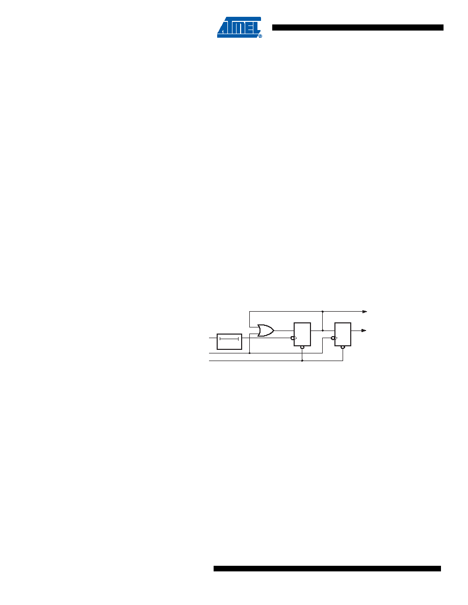
Start Condition Detector
The start condition detector is shown in Figure 13-6. The SDA line is delayed (in the range of 50
to 300 ns) to ensure valid sampling of the SCL line. The start condition detector is only enabled
in Two-wire mode.
Figure 13-6.
Start Condition Detector, Logic Diagram
The start condition detector works asynchronously and can therefore wake up the processor
from power-down sleep mode. However, the protocol used might have restrictions on the SCL
hold time. Therefore, when using this feature in this case the Oscillator start-up time set by the
CKSEL Fuses (see “Clock System” on page 24) must also be taken into the consideration. Refer
to the USISIF bit description on page Page 132 for further details.
13.3.6
Clock speed considerations
Maximum frequency for SCL and SCK is f
CK / 2. This is also the maximum data transmit and
receive rate in both two- and three-wire mode. In two-wire slave mode the Two-wire Clock Con-
trol Unit will hold the SCL low until the slave is ready to receive more data. This may reduce the
actual data rate in two-wire mode.
13.4
Alternative USI Usage
The flexible design of the USI allows it to be used for other tasks when serial communication is
not needed. Below are some examples.
SDA
SCL
Write( USISIF)
CLOCK
HOLD
USISIF
DQ
CLR
DQ
CLR
相关PDF资料 |
PDF描述 |
|---|---|
| PCA9671BS,118 | IC I/O EXPANDER I2C 16B 24HVQFN |
| ATTINY84A-CCUR | MCU AVR 8K FLASH 20MHZ 3X3UFBGA |
| ATTINY24A-MMHR | MCU AVR 2KB FLASH 20MHZ 20QFN |
| PCA9506BS,118 | IC I/O EXPANDER I2C 40B 56HVQFN |
| PCA8575PW,118 | IC I/O EXPANDER I2C 16B 24TSSOP |
相关代理商/技术参数 |
参数描述 |
|---|---|
| ATTINY261-ESMZ | 制造商:ATMEL 制造商全称:ATMEL Corporation 功能描述:8-bit Microcontroller with 2/4/8K Bytes In-System Programmable Flash |
| ATTINY261-ESSZ | 制造商:ATMEL 制造商全称:ATMEL Corporation 功能描述:8-bit Microcontroller with 2/4/8K Bytes In-System Programmable Flash |
| ATTINY261-ESXZ | 制造商:ATMEL 制造商全称:ATMEL Corporation 功能描述:8-bit Microcontroller with 2/4/8K Bytes In-System Programmable Flash |
| ATTINY261V | 制造商:ATMEL 制造商全称:ATMEL Corporation 功能描述:8-bit Microcontroller with 2/4/8K Bytes In-System Programmable Flash |
| ATTINY261V-10MU | 功能描述:8位微控制器 -MCU AVR 2K FLASH 128B EE 128B SRAM ADC RoHS:否 制造商:Silicon Labs 核心:8051 处理器系列:C8051F39x 数据总线宽度:8 bit 最大时钟频率:50 MHz 程序存储器大小:16 KB 数据 RAM 大小:1 KB 片上 ADC:Yes 工作电源电压:1.8 V to 3.6 V 工作温度范围:- 40 C to + 105 C 封装 / 箱体:QFN-20 安装风格:SMD/SMT |
发布紧急采购,3分钟左右您将得到回复。