- 您现在的位置:买卖IC网 > PDF目录11220 > ATTINY44A-MUR (Atmel)MCU AVR 4KB FLASH 20MHZ 20QFN PDF资料下载
参数资料
| 型号: | ATTINY44A-MUR |
| 厂商: | Atmel |
| 文件页数: | 4/135页 |
| 文件大小: | 0K |
| 描述: | MCU AVR 4KB FLASH 20MHZ 20QFN |
| 产品培训模块: | MCU Product Line Introduction tinyAVR Introduction |
| 标准包装: | 6,000 |
| 系列: | AVR® ATtiny |
| 核心处理器: | AVR |
| 芯体尺寸: | 8-位 |
| 速度: | 20MHz |
| 连通性: | USI |
| 外围设备: | 欠压检测/复位,POR,PWM,温度传感器,WDT |
| 输入/输出数: | 12 |
| 程序存储器容量: | 4KB(2K x 16) |
| 程序存储器类型: | 闪存 |
| EEPROM 大小: | 256 x 8 |
| RAM 容量: | 256 x 8 |
| 电压 - 电源 (Vcc/Vdd): | 1.8 V ~ 5.5 V |
| 数据转换器: | A/D 8x10b |
| 振荡器型: | 内部 |
| 工作温度: | -40°C ~ 85°C |
| 封装/外壳: | 20-WFQFN 裸露焊盘 |
| 包装: | 带卷 (TR) |
第1页第2页第3页当前第4页第5页第6页第7页第8页第9页第10页第11页第12页第13页第14页第15页第16页第17页第18页第19页第20页第21页第22页第23页第24页第25页第26页第27页第28页第29页第30页第31页第32页第33页第34页第35页第36页第37页第38页第39页第40页第41页第42页第43页第44页第45页第46页第47页第48页第49页第50页第51页第52页第53页第54页第55页第56页第57页第58页第59页第60页第61页第62页第63页第64页第65页第66页第67页第68页第69页第70页第71页第72页第73页第74页第75页第76页第77页第78页第79页第80页第81页第82页第83页第84页第85页第86页第87页第88页第89页第90页第91页第92页第93页第94页第95页第96页第97页第98页第99页第100页第101页第102页第103页第104页第105页第106页第107页第108页第109页第110页第111页第112页第113页第114页第115页第116页第117页第118页第119页第120页第121页第122页第123页第124页第125页第126页第127页第128页第129页第130页第131页第132页第133页第134页第135页
101
32015G–AVR32–09/09
AT32AP7001
NEXUS_ACCESS or a MEMORY_ACCESS JTAG command is loaded into the instruction regis-
ter before entering sleep mode some clocks are left running to enable debugging of the system.
This will increase the power consumption of the device. If the part entered static mode without a
NEXUS_ACCESS ot MEMORY_ACCESS instruction loaded into the JTAG instruction register
an external reset is the only way for the debugger to get the part out of the sleep mode.
When not debugging a program and using sleep modes the JTAG should always have the
IDCODE instruction loaded into the JTAG instruction register and the OCD system should be
disabled. Otherwise some clocks may be left running, increasing the power consumption.
11.5.7
Generic clocks
Timers, communication modules, and other modules connected to external circuitry may require
specific clock frequencies to operate correctly. The Power Manager contains an implementation
defined number of generic clocks, that can provide a wide range of accurate clock frequencies.
Each generic clock module runs from either Oscillator 0 or 1, or PLL0 or 1. The selected source
can optionally be divided by any even integer up to 512. Each clock can be independently
enabled and disabled, and is also automatically disabled along with peripheral clocks by the
Sleep Controller.
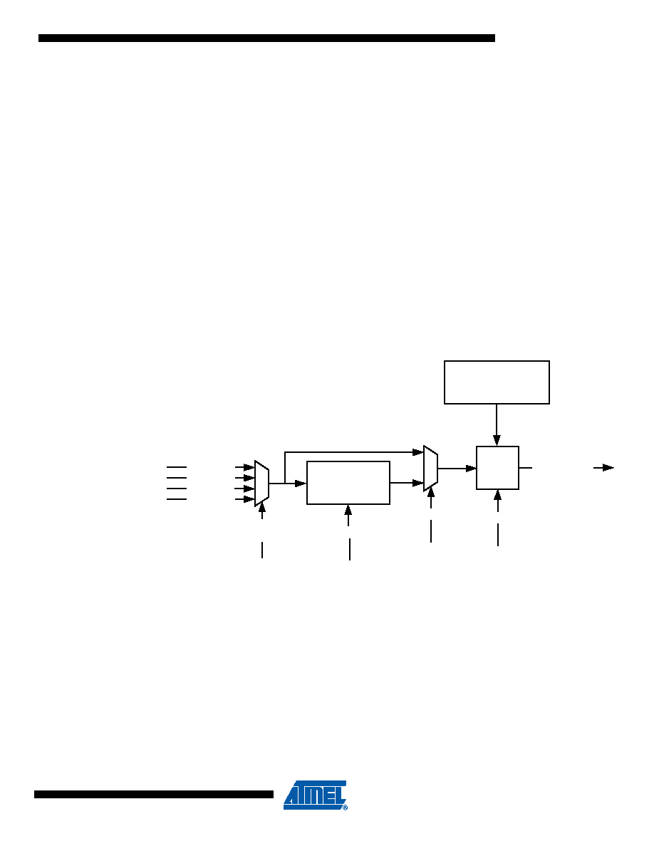
Figure 11-4. Generic clock generation
11.5.7.1
Enabling a generic clock
A generic clock is enabled by writing the CEN bit in GCCTRL to 1. Each generic clock can use
either Oscillator 0 or 1 or PLL0 or 1 as source, as selected by the PLLSEL and OSCSEL bits.
The source clock can optionally be divided by writing DIVEN to 1 and the division factor to DIV,
resulting in the output frequency:
f
GCLK = fSRC / (2*(DIV+1))
Divider
0
1
Osc0 clock
PLL0 clock
PLLSEL
OSCSEL
Osc1 clock
PLL1 clock
Generic Clock
DIV
0
1
DIVEN
Mask
CEN
Sleep
Controller
相关PDF资料 |
PDF描述 |
|---|---|
| VE-BW0-IX | CONVERTER MOD DC/DC 5V 75W |
| ADG513BNZ | IC SWITCH QUAD SPST 16DIP |
| ADG5412BRUZ | IC SWITCH QUAD SPST 16TSSOP |
| MB95F213KPH-G-SNE2 | IC MCU 8KB FLASH F2MC-8FX 8DIP |
| MB95F213KPF-G-SNE2 | IC MCU 8KB FLASH F2MC-8FX 8SOP |
相关代理商/技术参数 |
参数描述 |
|---|---|
| ATTINY44A-PU | 功能描述:8位微控制器 -MCU 1.8V, 20MHz Industrial Temp RoHS:否 制造商:Silicon Labs 核心:8051 处理器系列:C8051F39x 数据总线宽度:8 bit 最大时钟频率:50 MHz 程序存储器大小:16 KB 数据 RAM 大小:1 KB 片上 ADC:Yes 工作电源电压:1.8 V to 3.6 V 工作温度范围:- 40 C to + 105 C 封装 / 箱体:QFN-20 安装风格:SMD/SMT |
| ATTINY44A-SSF | 功能描述:8位微控制器 -MCU 4KB FL 256B EE 256B SRAM 20MHz Hi +125C RoHS:否 制造商:Silicon Labs 核心:8051 处理器系列:C8051F39x 数据总线宽度:8 bit 最大时钟频率:50 MHz 程序存储器大小:16 KB 数据 RAM 大小:1 KB 片上 ADC:Yes 工作电源电压:1.8 V to 3.6 V 工作温度范围:- 40 C to + 105 C 封装 / 箱体:QFN-20 安装风格:SMD/SMT |
| ATTINY44A-SSFR | 功能描述:8位微控制器 -MCU 4KB FL 256B EE 256B SRAM 20MHz Hi +125C RoHS:否 制造商:Silicon Labs 核心:8051 处理器系列:C8051F39x 数据总线宽度:8 bit 最大时钟频率:50 MHz 程序存储器大小:16 KB 数据 RAM 大小:1 KB 片上 ADC:Yes 工作电源电压:1.8 V to 3.6 V 工作温度范围:- 40 C to + 105 C 封装 / 箱体:QFN-20 安装风格:SMD/SMT |
| ATTINY44A-SSN | 功能描述:8位微控制器 -MCU 4K FLASH 256B EE 256B SRAM - 20MHz RoHS:否 制造商:Silicon Labs 核心:8051 处理器系列:C8051F39x 数据总线宽度:8 bit 最大时钟频率:50 MHz 程序存储器大小:16 KB 数据 RAM 大小:1 KB 片上 ADC:Yes 工作电源电压:1.8 V to 3.6 V 工作温度范围:- 40 C to + 105 C 封装 / 箱体:QFN-20 安装风格:SMD/SMT |
| ATTINY44A-SSNR | 功能描述:8位微控制器 -MCU AVR 4KB FL 256B EE 256B SRAM 20MHz 105C RoHS:否 制造商:Silicon Labs 核心:8051 处理器系列:C8051F39x 数据总线宽度:8 bit 最大时钟频率:50 MHz 程序存储器大小:16 KB 数据 RAM 大小:1 KB 片上 ADC:Yes 工作电源电压:1.8 V to 3.6 V 工作温度范围:- 40 C to + 105 C 封装 / 箱体:QFN-20 安装风格:SMD/SMT |
发布紧急采购,3分钟左右您将得到回复。