参数资料
| 型号: | ATTINY48-MUR |
| 厂商: | Atmel |
| 文件页数: | 59/302页 |
| 文件大小: | 0K |
| 描述: | MCU AVR 4KB FLASH 12MHZ 32QFN |
| 产品培训模块: | tinyAVR Introduction |
| 标准包装: | 6,000 |
| 系列: | AVR® ATtiny |
| 核心处理器: | AVR |
| 芯体尺寸: | 8-位 |
| 速度: | 12MHz |
| 连通性: | I²C,SPI |
| 外围设备: | 欠压检测/复位,POR,WDT |
| 输入/输出数: | 28 |
| 程序存储器容量: | 4KB(2K x 16) |
| 程序存储器类型: | 闪存 |
| EEPROM 大小: | 64 x 8 |
| RAM 容量: | 256 x 8 |
| 电压 - 电源 (Vcc/Vdd): | 1.8 V ~ 5.5 V |
| 数据转换器: | A/D 8x10b |
| 振荡器型: | 内部 |
| 工作温度: | -40°C ~ 85°C |
| 封装/外壳: | 32-VFQFN 裸露焊盘 |
| 包装: | 带卷 (TR) |
| 其它名称: | ATTINY48-MUR-ND |
第1页第2页第3页第4页第5页第6页第7页第8页第9页第10页第11页第12页第13页第14页第15页第16页第17页第18页第19页第20页第21页第22页第23页第24页第25页第26页第27页第28页第29页第30页第31页第32页第33页第34页第35页第36页第37页第38页第39页第40页第41页第42页第43页第44页第45页第46页第47页第48页第49页第50页第51页第52页第53页第54页第55页第56页第57页第58页当前第59页第60页第61页第62页第63页第64页第65页第66页第67页第68页第69页第70页第71页第72页第73页第74页第75页第76页第77页第78页第79页第80页第81页第82页第83页第84页第85页第86页第87页第88页第89页第90页第91页第92页第93页第94页第95页第96页第97页第98页第99页第100页第101页第102页第103页第104页第105页第106页第107页第108页第109页第110页第111页第112页第113页第114页第115页第116页第117页第118页第119页第120页第121页第122页第123页第124页第125页第126页第127页第128页第129页第130页第131页第132页第133页第134页第135页第136页第137页第138页第139页第140页第141页第142页第143页第144页第145页第146页第147页第148页第149页第150页第151页第152页第153页第154页第155页第156页第157页第158页第159页第160页第161页第162页第163页第164页第165页第166页第167页第168页第169页第170页第171页第172页第173页第174页第175页第176页第177页第178页第179页第180页第181页第182页第183页第184页第185页第186页第187页第188页第189页第190页第191页第192页第193页第194页第195页第196页第197页第198页第199页第200页第201页第202页第203页第204页第205页第206页第207页第208页第209页第210页第211页第212页第213页第214页第215页第216页第217页第218页第219页第220页第221页第222页第223页第224页第225页第226页第227页第228页第229页第230页第231页第232页第233页第234页第235页第236页第237页第238页第239页第240页第241页第242页第243页第244页第245页第246页第247页第248页第249页第250页第251页第252页第253页第254页第255页第256页第257页第258页第259页第260页第261页第262页第263页第264页第265页第266页第267页第268页第269页第270页第271页第272页第273页第274页第275页第276页第277页第278页第279页第280页第281页第282页第283页第284页第285页第286页第287页第288页第289页第290页第291页第292页第293页第294页第295页第296页第297页第298页第299页第300页第301页第302页
151
8008H–AVR–04/11
ATtiny48/88
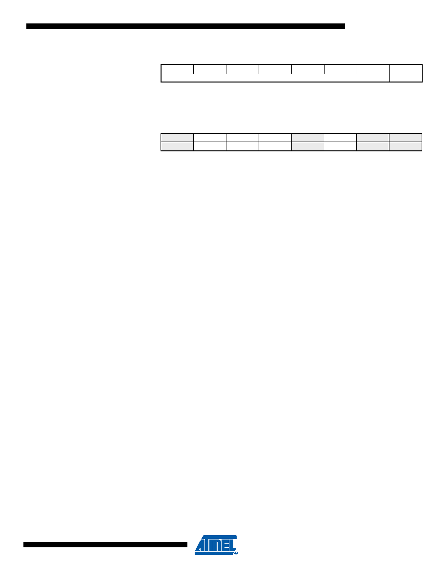
To initiate the Slave Transmitter mode, TWAR and TWCR must be initialized as follows:
The upper seven bits are the address to which the 2-wire Serial Interface will respond when
addressed by a Master. If the LSB is set, the TWI will respond to the general call address (0x00),
otherwise it will ignore the general call address.
TWEN must be written to one to enable the TWI. The TWEA bit must be written to one to enable
the acknowledgement of the device’s own slave address or the general call address. TWSTA
and TWSTO must be written to zero.
When TWAR and TWCR have been initialized, the TWI waits until it is addressed by its own
slave address (or the general call address if enabled) followed by the data direction bit. If the
direction bit is “1” (read), the TWI will operate in ST mode, otherwise SR mode is entered. After
its own slave address and the write bit have been received, the TWINT Flag is set and a valid
status code can be read from TWSR. The status code is used to determine the appropriate soft-
ware action. The appropriate action to be taken for each status code is detailed in Table 15-5.
The Slave Transmitter mode may also be entered if arbitration is lost while the TWI is in the
Master mode (see state 0xB0).
If the TWEA bit is written to zero during a transfer, the TWI will transmit the last byte of the trans-
fer. State 0xC0 or state 0xC8 will be entered, depending on whether the Master Receiver
transmits a NACK or ACK after the final byte. The TWI is switched to the not addressed Slave
mode, and will ignore the Master if it continues the transfer. Thus the Master Receiver receives
all “1” as serial data. State 0xC8 is entered if the Master demands additional data bytes (by
transmitting ACK), even though the Slave has transmitted the last byte (TWEA zero and expect-
ing NACK from the Master).
While TWEA is zero, the TWI does not respond to its own slave address. However, the 2-wire
Serial Bus is still monitored and address recognition may resume at any time by setting TWEA.
This implies that the TWEA bit may be used to temporarily isolate the TWI from the 2-wire Serial
Bus.
In all sleep modes other than Idle mode, the clock system to the TWI is turned off. If the TWEA
bit is set, the interface can still acknowledge its own slave address or the general call address by
using the 2-wire Serial Bus clock as a clock source. The part will then wake up from sleep and
the TWI will hold the SCL clock will low during the wake up and until the TWINT Flag is cleared
(by writing it to one). Further data transmission will be carried out as normal, with the AVR clocks
running as normal. Observe that if the AVR is set up with a long start-up time, the SCL line may
be held low for a long time, blocking other data transmissions.
Note that the 2-wire Serial Interface Data Register – TWDR does not reflect the last byte present
on the bus when waking up from these sleep modes.
TWAR
TWA6
TWA5
TWA4
TWA3
TWA2
TWA1
TWA0
TWGCE
value
Device’s Own Slave Address
TWCR
TWINT
TWEA
TWSTA
TWSTO
TWWC
TWEN
–
TWIE
value
0
100
01
0
X
相关PDF资料 |
PDF描述 |
|---|---|
| ATTINY13A-MU | IC MCU AVR 1K FLASH 20MHZ 20-QFN |
| ATTINY13A-SN | IC MCU AVR 1KB FLASH 20MHZ 8SOIC |
| ATTINY13A-SH | IC MCU AVR 1K FLASH 20MHZ 8SOIC |
| ATTINY13A-SSH | IC MCU AVR 1K FLASH 20MHZ 8SOIC |
| ATTINY13A-SSU | IC MCU AVR 1K FLASH 20MHZ 8SOIC |
相关代理商/技术参数 |
参数描述 |
|---|---|
| ATTINY48PRE | 制造商:ATMEL 制造商全称:ATMEL Corporation 功能描述:123 Powerful Instructions – Most Single Clock Cycle Execution |
| ATTINY48-PU | 功能描述:8位微控制器 -MCU 4KB In-system Flash 12MHz 1.8V-5.5V RoHS:否 制造商:Silicon Labs 核心:8051 处理器系列:C8051F39x 数据总线宽度:8 bit 最大时钟频率:50 MHz 程序存储器大小:16 KB 数据 RAM 大小:1 KB 片上 ADC:Yes 工作电源电压:1.8 V to 3.6 V 工作温度范围:- 40 C to + 105 C 封装 / 箱体:QFN-20 安装风格:SMD/SMT |
| ATTINY48V-W | 功能描述:8位微控制器 -MCU Microcontroller RoHS:否 制造商:Silicon Labs 核心:8051 处理器系列:C8051F39x 数据总线宽度:8 bit 最大时钟频率:50 MHz 程序存储器大小:16 KB 数据 RAM 大小:1 KB 片上 ADC:Yes 工作电源电压:1.8 V to 3.6 V 工作温度范围:- 40 C to + 105 C 封装 / 箱体:QFN-20 安装风格:SMD/SMT |
| ATTINY48V-W-11 | 功能描述:8位微控制器 -MCU Microcontroller RoHS:否 制造商:Silicon Labs 核心:8051 处理器系列:C8051F39x 数据总线宽度:8 bit 最大时钟频率:50 MHz 程序存储器大小:16 KB 数据 RAM 大小:1 KB 片上 ADC:Yes 工作电源电压:1.8 V to 3.6 V 工作温度范围:- 40 C to + 105 C 封装 / 箱体:QFN-20 安装风格:SMD/SMT |
| ATTINY48-W-11 | 功能描述:8位微控制器 -MCU Microcontroller RoHS:否 制造商:Silicon Labs 核心:8051 处理器系列:C8051F39x 数据总线宽度:8 bit 最大时钟频率:50 MHz 程序存储器大小:16 KB 数据 RAM 大小:1 KB 片上 ADC:Yes 工作电源电压:1.8 V to 3.6 V 工作温度范围:- 40 C to + 105 C 封装 / 箱体:QFN-20 安装风格:SMD/SMT |
发布紧急采购,3分钟左右您将得到回复。