- 您现在的位置:买卖IC网 > PDF目录11217 > ATTINY84-20MUR (Atmel)MCU AVR 8KB FLASH 20MHZ 20QFN PDF资料下载
参数资料
| 型号: | ATTINY84-20MUR |
| 厂商: | Atmel |
| 文件页数: | 41/238页 |
| 文件大小: | 0K |
| 描述: | MCU AVR 8KB FLASH 20MHZ 20QFN |
| 产品培训模块: | tinyAVR Introduction |
| 标准包装: | 6,000 |
| 系列: | AVR® ATtiny |
| 核心处理器: | AVR |
| 芯体尺寸: | 8-位 |
| 速度: | 20MHz |
| 连通性: | USI |
| 外围设备: | 欠压检测/复位,POR,PWM,温度传感器,WDT |
| 输入/输出数: | 12 |
| 程序存储器容量: | 8KB(4K x 16) |
| 程序存储器类型: | 闪存 |
| EEPROM 大小: | 512 x 8 |
| RAM 容量: | 512 x 8 |
| 电压 - 电源 (Vcc/Vdd): | 2.7 V ~ 5.5 V |
| 数据转换器: | A/D 8x10b |
| 振荡器型: | 内部 |
| 工作温度: | -40°C ~ 85°C |
| 封装/外壳: | 20-WFQFN 裸露焊盘 |
| 包装: | 带卷 (TR) |
第1页第2页第3页第4页第5页第6页第7页第8页第9页第10页第11页第12页第13页第14页第15页第16页第17页第18页第19页第20页第21页第22页第23页第24页第25页第26页第27页第28页第29页第30页第31页第32页第33页第34页第35页第36页第37页第38页第39页第40页当前第41页第42页第43页第44页第45页第46页第47页第48页第49页第50页第51页第52页第53页第54页第55页第56页第57页第58页第59页第60页第61页第62页第63页第64页第65页第66页第67页第68页第69页第70页第71页第72页第73页第74页第75页第76页第77页第78页第79页第80页第81页第82页第83页第84页第85页第86页第87页第88页第89页第90页第91页第92页第93页第94页第95页第96页第97页第98页第99页第100页第101页第102页第103页第104页第105页第106页第107页第108页第109页第110页第111页第112页第113页第114页第115页第116页第117页第118页第119页第120页第121页第122页第123页第124页第125页第126页第127页第128页第129页第130页第131页第132页第133页第134页第135页第136页第137页第138页第139页第140页第141页第142页第143页第144页第145页第146页第147页第148页第149页第150页第151页第152页第153页第154页第155页第156页第157页第158页第159页第160页第161页第162页第163页第164页第165页第166页第167页第168页第169页第170页第171页第172页第173页第174页第175页第176页第177页第178页第179页第180页第181页第182页第183页第184页第185页第186页第187页第188页第189页第190页第191页第192页第193页第194页第195页第196页第197页第198页第199页第200页第201页第202页第203页第204页第205页第206页第207页第208页第209页第210页第211页第212页第213页第214页第215页第216页第217页第218页第219页第220页第221页第222页第223页第224页第225页第226页第227页第228页第229页第230页第231页第232页第233页第234页第235页第236页第237页第238页
2001 Microchip Technology Inc.
DS39026C-page 133
PIC18CXX2
14.4.2
GENERAL CALL ADDRESS
SUPPORT
The addressing procedure for the I2C bus is such that
the first byte after the START condition usually deter-
mines which device will be the slave addressed by the
master. The exception is the general call address which
can address all devices. When this address is used, all
devices should, in theory, respond with an acknowl-
edge.
The general call address is one of eight addresses
reserved for specific purposes by the I2C protocol. It
consists of all 0’s with R/W = 0.
The general call address is recognized when the Gen-
eral Call Enable bit (GCEN) is enabled (SSPCON2<7>
is set). Following a START bit detect, 8-bits are shifted
into the SSPSR and the address is compared against
the SSPADD. It is also compared to the general call
address and fixed in hardware.
If the general call address matches, the SSPSR is
transferred to the SSPBUF, the BF flag bit is set (eighth
bit), and on the falling edge of the ninth bit (ACK bit),
the SSPIF interrupt flag bit is set.
When the interrupt is serviced, the source for the inter-
rupt can be checked by reading the contents of the
SSPBUF. The value can be used to determine if the
address was device specific or a general call address.
In 10-bit mode, the SSPADD is required to be updated
for the second half of the address to match, and the UA
bit is set (SSPSTAT<1>). If the general call address is
sampled when the GCEN bit is set, while the slave is
configured in 10-bit address mode, then the second
half of the address is not necessary, the UA bit will not
be set, and the slave will begin receiving data after the
Acknowledge (Figure 14-12).
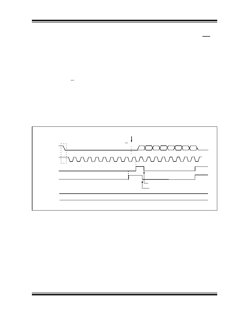
FIGURE 14-12:
SLAVE MODE GENERAL CALL ADDRESS SEQUENCE
(7 OR 10-BIT ADDRESS MODE)
14.4.3
MASTER MODE
Master mode of operation is supported by interrupt
generation on the detection of the START and STOP
conditions. The STOP (P) and START (S) bits are
cleared from a RESET or when the MSSP module is
disabled. Control of the I2C bus may be taken when the
P bit is set, or the bus is idle, with both the S and P bits
clear.
In Master mode, the SCL and SDA lines are manipu-
lated by the MSSP hardware.
The following events will cause SSP Interrupt Flag bit,
SSPIF, to be set (SSP interrupt, if enabled):
START condition
STOP condition
Data transfer byte transmitted/received
Acknowledge Transmit
Repeated START
SDA
SCL
S
SSPIF
BF (SSPSTAT<0>)
SSPOV (SSPCON1<6>)
Cleared in software
SSPBUF is read
R/W = 0
ACK
General Call Address
Address is compared to General Call Address
GCEN (SSPCON2<7>)
Receiving Data
ACK
12
3
4
5
6
7
8
9
1
2
3
4
5
67
8
9
D7
D6
D5
D4
D3
D2
D1
D0
after ACK, set interrupt
’0’
’1’
相关PDF资料 |
PDF描述 |
|---|---|
| ATTINY26L-8MUR | IC MCU AVR 2K 5V 8MHZ 32QFN |
| VE-B2V-IX-F1 | CONVERTER MOD DC/DC 5.8V 75W |
| ATTINY26-16MUR | IC MCU AVR 2K 16MHZ IND 32QFN |
| VE-B2V-IW-F4 | CONVERTER MOD DC/DC 5.8V 100W |
| VE-B2V-IW-F3 | CONVERTER MOD DC/DC 5.8V 100W |
相关代理商/技术参数 |
参数描述 |
|---|---|
| ATTINY84-20PU | 功能描述:8位微控制器 -MCU 8kB Flash 0.512kB EEPROM 12 I/O Pins RoHS:否 制造商:Silicon Labs 核心:8051 处理器系列:C8051F39x 数据总线宽度:8 bit 最大时钟频率:50 MHz 程序存储器大小:16 KB 数据 RAM 大小:1 KB 片上 ADC:Yes 工作电源电压:1.8 V to 3.6 V 工作温度范围:- 40 C to + 105 C 封装 / 箱体:QFN-20 安装风格:SMD/SMT |
| ATTINY84-20SSU | 功能描述:8位微控制器 -MCU 8-bit 512B SRAM 20MHz 2.7-5.5V RoHS:否 制造商:Silicon Labs 核心:8051 处理器系列:C8051F39x 数据总线宽度:8 bit 最大时钟频率:50 MHz 程序存储器大小:16 KB 数据 RAM 大小:1 KB 片上 ADC:Yes 工作电源电压:1.8 V to 3.6 V 工作温度范围:- 40 C to + 105 C 封装 / 箱体:QFN-20 安装风格:SMD/SMT |
| ATTINY84-20SSUR | 功能描述:8位微控制器 -MCU AVR 8KB FLSH 512B EE 512B SRAM-10MHz, IND RoHS:否 制造商:Silicon Labs 核心:8051 处理器系列:C8051F39x 数据总线宽度:8 bit 最大时钟频率:50 MHz 程序存储器大小:16 KB 数据 RAM 大小:1 KB 片上 ADC:Yes 工作电源电压:1.8 V to 3.6 V 工作温度范围:- 40 C to + 105 C 封装 / 箱体:QFN-20 安装风格:SMD/SMT |
| ATTINY84A | 制造商:ATMEL 制造商全称:ATMEL Corporation 功能描述:8-bit Microcontroller with 2K/4K/8K Bytes In-System Programmable Flash |
| ATTINY84A-CCU | 功能描述:8位微控制器 -MCU 20MHz Ind. Grade RoHS:否 制造商:Silicon Labs 核心:8051 处理器系列:C8051F39x 数据总线宽度:8 bit 最大时钟频率:50 MHz 程序存储器大小:16 KB 数据 RAM 大小:1 KB 片上 ADC:Yes 工作电源电压:1.8 V to 3.6 V 工作温度范围:- 40 C to + 105 C 封装 / 箱体:QFN-20 安装风格:SMD/SMT |
发布紧急采购,3分钟左右您将得到回复。