- 您现在的位置:买卖IC网 > PDF目录378409 > ATW2805S (International Rectifier) ADVANCED ANALOG HYBRID-HIGH RELIABILITY DC/DC CONVERTERS PDF资料下载
参数资料
| 型号: | ATW2805S |
| 厂商: | International Rectifier |
| 英文描述: | ADVANCED ANALOG HYBRID-HIGH RELIABILITY DC/DC CONVERTERS |
| 中文描述: | 先进的模拟混合,高度可靠的DC / DC转换器 |
| 文件页数: | 5/8页 |
| 文件大小: | 58K |
| 代理商: | ATW2805S |

www.irf.com
5
ATW28XXD Series
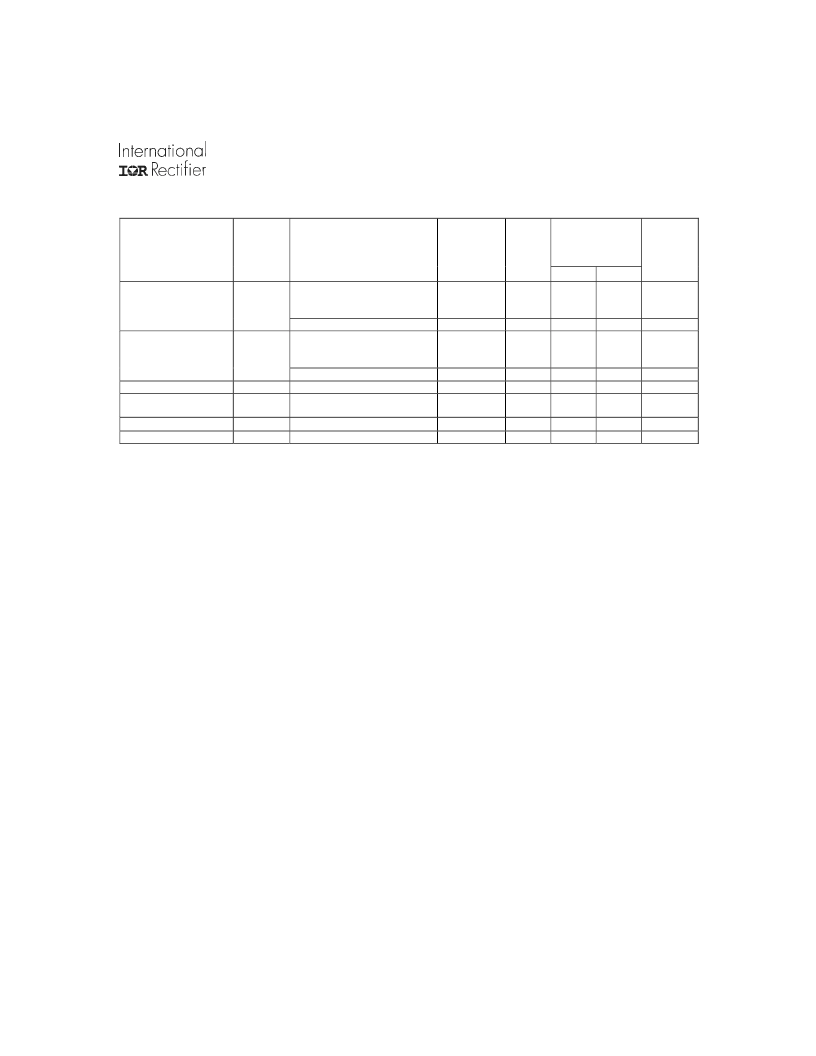
Table II. Electrical Performance Characteristics -
continued
Notes to Specifications
ATW2815D
1 Recovery time is measured from the initiation of the transient to where V
has returned to within
±
1% of V
at 50% load.
2 Turn-on delay time measurement is for either a step application of power at the input or the removal of a ground signal from the
inhibit pin (pin 8) while power is applied to the input.
3 An overload is that condition with a load in excess of the rated load but less than that necessary to trigger the short circuit
protection and is the condition of maximum power dissipation.
4 Above +125
°
C case, derate output power linearly to 0 at +135
°
C case.
5 Input step transition time between 2 and 10 microseconds.
6 Capacitive load may be any value from 0 to the maximum limit without compromising DC performance. A capacitive load in
excess of the maximum limit will not disturb loop stability but will interfere with the operation of the load fault detection circuitry,
appearing as a short circuit during turn on.
7 Load step transition time between 2 and 10 microseconds.
8 Bandwidth guaranteed by design. Tested for 20KHz to 2MHz.
9 Load current split equally between +V
and –V
.
10 When operating with unbalanced loads, at least 25% of the load must be on the positive output to maintain regulation.
11 Parameter guaranteed by line and load regulation tests.
12 Parameter shall be tested as part of design characterization and after design or process changes. Thereafter parameters shall be
guaranteed to the limits specified in Table II.
13 Up to 90% of full power is available from either output provided the total output does not exceed 30 watts.
Test
Symbol
Conditions
-55°C
≤
Tc
≤
+125°C
Vin = 28 Vdc ±5%, C
= 0
unless otherwise specified
Input step from/to 18 to
40VDC
Group A
Subgroups
Device
Types
Limits
Unit
Min
Max
+180
Output response
transient step line
changes
Recovery time
transient step line
changes
Turn on overshoot
Turn on delay
VO
TLINE
4,5,6
All
mV pk
Input step from 40 to18 VDC
Input step from/to 18 to 40
VDC
4,5,6
4,5,6
All
All
-600
400
mV pk
μ
s
TT
LINE
Input step from 40 to 18 VDC
I
OUT
=
0 and 2000mA
I
OUT
= 0 and 2000mA
V
IN
= 18 to 40 VDC
Flange
4,5,6
4,5,6
4,5,6
All
All
All
400
750
12
μ
s
VTon
OS
Ton
D
mV pk
ms
2
Load fault recovery
Weight
12
Tr
LF
4,5,6
All
12
75
ms
grams
相关PDF资料 |
PDF描述 |
|---|---|
| ATW2812D | ADVANCED ANALOG HYBRID-HIGH RELIABILITY DC/DC CONVERTERS |
| ATXP6 | Jumper Free Over Clock Controller |
| ATXP6G | Jumper Free Over Clock Controller |
| AU5517DR2 | Dual Operational Transconductance Amplifier |
| AU5517DR2G | Dual Operational Transconductance Amplifier |
相关代理商/技术参数 |
参数描述 |
|---|---|
| ATW2805S/CH | 制造商:International Rectifier 功能描述:Module DC-DC 1-OUT 5V 6A 30W 10-Pin ATW 制造商:International Rectifier 功能描述:DC/DC CONVERTER, FLANGED, CLASS H - Bulk |
| ATW2805S/CH-MSTR | 制造商:International Rectifier 功能描述:DC/DC CONVERTER, FLANGED, CLASS H, MASTER - Tape and Reel |
| ATW2805S/CH-SLV | 制造商:International Rectifier 功能描述:DC/DC CONVERTER, FLANGED, CLASS H, SLAVE - Bulk |
| ATW2805S/ES | 制造商:International Rectifier 功能描述:Module DC-DC 1-OUT 5V 6A 30W 10-Pin ATW 制造商:International Rectifier 功能描述:DC/DC CONVERTER, FLANGED, ENVIRONMENTAL SCREENING - Bulk |
| ATW2805S/ES-MSTR | 制造商:International Rectifier 功能描述:DC/DC CONVERTER, FLANGED, ENVIRONMENTAL SCREENING, MASTER - Tape and Reel |
发布紧急采购,3分钟左右您将得到回复。