- 您现在的位置:买卖IC网 > PDF目录11203 > ATXMEGA256A3B-MHR (Atmel)IC MCU 8BIT 256KB FLASH 64VQFN PDF资料下载
参数资料
| 型号: | ATXMEGA256A3B-MHR |
| 厂商: | Atmel |
| 文件页数: | 176/287页 |
| 文件大小: | 0K |
| 描述: | IC MCU 8BIT 256KB FLASH 64VQFN |
| 标准包装: | 4,000 |
| 系列: | AVR® XMEGA |
| 核心处理器: | AVR |
| 芯体尺寸: | 8/16-位 |
| 速度: | 32MHz |
| 连通性: | I²C,SPI,UART/USART |
| 外围设备: | 欠压检测/复位,DMA,POR,PWM,WDT |
| 输入/输出数: | 49 |
| 程序存储器容量: | 256KB(128K x 16) |
| 程序存储器类型: | 闪存 |
| EEPROM 大小: | 4K x 8 |
| RAM 容量: | 16K x 8 |
| 电压 - 电源 (Vcc/Vdd): | 1.6 V ~ 3.6 V |
| 数据转换器: | A/D 16x12b; D/A 2x12b |
| 振荡器型: | 内部 |
| 工作温度: | -40°C ~ 85°C |
| 封装/外壳: | 64-VFQFN 裸露焊盘 |
| 包装: | 带卷 (TR) |
| 配用: | ATSTK600-RC14-ND - STK600 SOCKET/ADAPTER 64TQFP |
第1页第2页第3页第4页第5页第6页第7页第8页第9页第10页第11页第12页第13页第14页第15页第16页第17页第18页第19页第20页第21页第22页第23页第24页第25页第26页第27页第28页第29页第30页第31页第32页第33页第34页第35页第36页第37页第38页第39页第40页第41页第42页第43页第44页第45页第46页第47页第48页第49页第50页第51页第52页第53页第54页第55页第56页第57页第58页第59页第60页第61页第62页第63页第64页第65页第66页第67页第68页第69页第70页第71页第72页第73页第74页第75页第76页第77页第78页第79页第80页第81页第82页第83页第84页第85页第86页第87页第88页第89页第90页第91页第92页第93页第94页第95页第96页第97页第98页第99页第100页第101页第102页第103页第104页第105页第106页第107页第108页第109页第110页第111页第112页第113页第114页第115页第116页第117页第118页第119页第120页第121页第122页第123页第124页第125页第126页第127页第128页第129页第130页第131页第132页第133页第134页第135页第136页第137页第138页第139页第140页第141页第142页第143页第144页第145页第146页第147页第148页第149页第150页第151页第152页第153页第154页第155页第156页第157页第158页第159页第160页第161页第162页第163页第164页第165页第166页第167页第168页第169页第170页第171页第172页第173页第174页第175页当前第176页第177页第178页第179页第180页第181页第182页第183页第184页第185页第186页第187页第188页第189页第190页第191页第192页第193页第194页第195页第196页第197页第198页第199页第200页第201页第202页第203页第204页第205页第206页第207页第208页第209页第210页第211页第212页第213页第214页第215页第216页第217页第218页第219页第220页第221页第222页第223页第224页第225页第226页第227页第228页第229页第230页第231页第232页第233页第234页第235页第236页第237页第238页第239页第240页第241页第242页第243页第244页第245页第246页第247页第248页第249页第250页第251页第252页第253页第254页第255页第256页第257页第258页第259页第260页第261页第262页第263页第264页第265页第266页第267页第268页第269页第270页第271页第272页第273页第274页第275页第276页第277页第278页第279页第280页第281页第282页第283页第284页第285页第286页第287页
2011 Microchip Technology Inc.
DS39932D-page 357
PIC18F46J11 FAMILY
21.2
Selecting and Configuring
Automatic Acquisition Time
The ADCON1 register allows the user to select an
acquisition time that occurs each time the GO/DONE
bit is set.
When the GO/DONE bit is set, sampling is stopped and
a conversion begins. The user is responsible for ensur-
ing the required acquisition time has passed between
selecting the desired input channel and setting the
GO/DONE bit. This occurs when the ACQT<2:0> bits
(ADCON1<5:3>) remain in their Reset state (‘000’) and
is compatible with devices that do not offer
programmable acquisition times.
If desired, the ACQT bits can be set to select a pro-
grammable acquisition time for the A/D module. When
the GO/DONE bit is set, the A/D module continues to
sample the input for the selected acquisition time, then
automatically begins a conversion. Since the acquisi-
tion time is programmed, there may be no need to wait
for an acquisition time between selecting a channel and
setting the GO/DONE bit.
In either case, when the conversion is completed, the
GO/DONE bit is cleared, the ADIF flag is set and the
A/D begins sampling the currently selected channel
again. If an acquisition time is programmed, there is
nothing to indicate if the acquisition time has ended or
if the conversion has begun.
21.3
Selecting the A/D Conversion
Clock
The A/D conversion time per bit is defined as TAD. The
A/D conversion requires 11 TAD per 10-bit conversion.
The source of the A/D conversion clock is software
selectable.
There are seven possible options for TAD:
2 TOSC
4 TOSC
8 TOSC
16 TOSC
32 TOSC
64 TOSC
Internal RC Oscillator
For correct A/D conversions, the A/D conversion clock
(TAD) must be as short as possible but greater than the
more information).
from the device operating frequencies and the A/D
clock source selected.
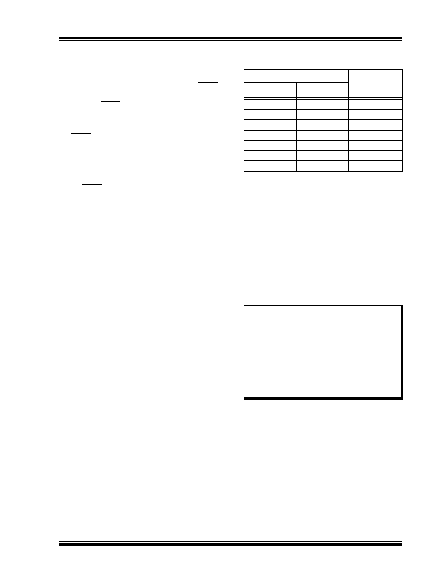
TABLE 21-1:
TAD vs. DEVICE OPERATING
FREQUENCIES
21.4
Configuring Analog Port Pins
The ANCON0, ANCON1 and TRISA registers control
the operation of the A/D port pins. The port pins needed
as analog inputs must have their corresponding TRIS
bits set (input). If the TRIS bit is cleared (output), the
digital output level (VOH or VOL) will be converted.
The A/D operation is independent of the state of the
CHS<3:0> bits and the TRIS bits.
AD Clock Source (TAD)Maximum
Device
Frequency
Operation
ADCS<2:0>
2 TOSC
000
2.86 MHz
4 TOSC
100
5.71 MHz
8 TOSC
001
11.43 MHz
16 TOSC
101
22.86 MHz
32 TOSC
010
45.71 MHz
64 TOSC
110
48.0 MHz
RC(2)
011
1.00 MHz(1)
Note 1:
The RC source has a typical TAD time of
4
s.
2:
For device frequencies above 1 MHz, the
device must be in Sleep mode for the
entire conversion or the A/D accuracy may
be out of specification.
Note 1:
When reading the PORT register, all pins
configured as analog input channels will
read as cleared (a low level). Pins config-
ured as digital inputs will convert an
analog input. Analog levels on a digitally
configured input will be accurately
converted.
2:
Analog levels on any pin defined as a
digital input may cause the digital input
buffer to consume current out of the
device’s specification limits.
相关PDF资料 |
PDF描述 |
|---|---|
| ATXMEGA256A3B-AUR | IC MCU 8BIT 256KB FLASH 64TQFP |
| VE-B33-IX-F2 | CONVERTER MOD DC/DC 24V 75W |
| VE-B33-IW-F4 | CONVERTER MOD DC/DC 24V 100W |
| AS1753S-T | IC SWITCH QUAD SPST 14-TSSOP |
| AS1752S-T | IC SWITCH QUAD SPST 14-TSSOP |
相关代理商/技术参数 |
参数描述 |
|---|---|
| ATXMEGA256A3B-MU | 制造商:Atmel Corporation 功能描述:MCU 8-Bit/16-Bit XMEGA AVR RISC 256KB Flash 1.8V/2.5V/3.3V 64-Pin QFN EP |
| ATXMEGA256A3BU-AN | 功能描述:AVR AVR? XMEGA? A3BU Microcontroller IC 8/16-Bit 32MHz 256KB (128K x 16) FLASH 制造商:atmel 系列:AVR? XMEGA? A3BU 包装:* 零件状态:有效 核心处理器:AVR 核心尺寸:8/16-位 速度:32MHz 连接性:I2C,IrDA,SPI,UART/USART,USB 外设:欠压检测/复位,DMA,POR,PWM,WDT I/O 数:47 程序存储容量:256KB(128K x 16) 程序存储器类型:闪存 EEPROM 容量:4K x 8 RAM 容量:16K x 8 电压 - 电源(Vcc/Vdd):1.6 V ~ 3.6 V 数据转换器:A/D 16x12b;D/A 2x12b 振荡器类型:内部 工作温度:-40°C ~ 105°C(TA) 封装/外壳:* 供应商器件封装:* 标准包装:160 |
| ATXMEGA256A3BU-ANR | 功能描述:AVR AVR? XMEGA? A3BU Microcontroller IC 8/16-Bit 32MHz 256KB (128K x 16) FLASH 制造商:atmel 系列:AVR? XMEGA? A3BU 包装:* 零件状态:有效 核心处理器:AVR 核心尺寸:8/16-位 速度:32MHz 连接性:I2C,IrDA,SPI,UART/USART,USB 外设:欠压检测/复位,DMA,POR,PWM,WDT I/O 数:47 程序存储容量:256KB(128K x 16) 程序存储器类型:闪存 EEPROM 容量:4K x 8 RAM 容量:16K x 8 电压 - 电源(Vcc/Vdd):1.6 V ~ 3.6 V 数据转换器:A/D 16x12b;D/A 2x12b 振荡器类型:内部 工作温度:-40°C ~ 105°C(TA) 封装/外壳:* 供应商器件封装:* 标准包装:2,000 |
| ATXMEGA256A3BU-AU | 功能描述:8位微控制器 -MCU AVR8 256KB FLSH 16KB RoHS:否 制造商:Silicon Labs 核心:8051 处理器系列:C8051F39x 数据总线宽度:8 bit 最大时钟频率:50 MHz 程序存储器大小:16 KB 数据 RAM 大小:1 KB 片上 ADC:Yes 工作电源电压:1.8 V to 3.6 V 工作温度范围:- 40 C to + 105 C 封装 / 箱体:QFN-20 安装风格:SMD/SMT |
| ATXMEGA256A3BU-AUR | 功能描述:AVR AVR? XMEGA? A3BU Microcontroller IC 8/16-Bit 32MHz 256KB (128K x 16) FLASH 64-TQFP (14x14) 制造商:atmel 系列:AVR? XMEGA? A3BU 包装:剪切带(CT) 零件状态:停产 核心处理器:AVR 核心尺寸:8/16-位 速度:32MHz 连接性:I2C,IrDA,SPI,UART/USART,USB 外设:欠压检测/复位,DMA,POR,PWM,WDT I/O 数:47 程序存储容量:256KB(128K x 16) 程序存储器类型:闪存 EEPROM 容量:4K x 8 RAM 容量:16K x 8 电压 - 电源(Vcc/Vdd):1.6 V ~ 3.6 V 数据转换器:A/D 16x12b;D/A 2x12b 振荡器类型:内部 工作温度:-40°C ~ 85°C(TA) 封装/外壳:64-TQFP 供应商器件封装:64-TQFP(14x14) 标准包装:1 |
发布紧急采购,3分钟左右您将得到回复。