- 您现在的位置:买卖IC网 > PDF目录17538 > AUIRS2110STR (International Rectifier)IC DRIVER HIGH/LOW SIDE 16SOIC PDF资料下载
参数资料
| 型号: | AUIRS2110STR |
| 厂商: | International Rectifier |
| 文件页数: | 5/18页 |
| 文件大小: | 0K |
| 描述: | IC DRIVER HIGH/LOW SIDE 16SOIC |
| 标准包装: | 1,000 |
| 配置: | 高端和低端,独立 |
| 输入类型: | 非反相 |
| 延迟时间: | 140ns |
| 电流 - 峰: | 2.5A |
| 配置数: | 1 |
| 输出数: | 2 |
| 高端电压 - 最大(自引导启动): | 500V |
| 电源电压: | 3 V ~ 20 V |
| 工作温度: | -40°C ~ 125°C |
| 安装类型: | 表面贴装 |
| 封装/外壳: | 16-SOIC(0.295",7.50mm 宽) |
| 供应商设备封装: | 16-SOIC |
| 包装: | 带卷 (TR) |
�� �
�
�AUIRS211(0,3)S�
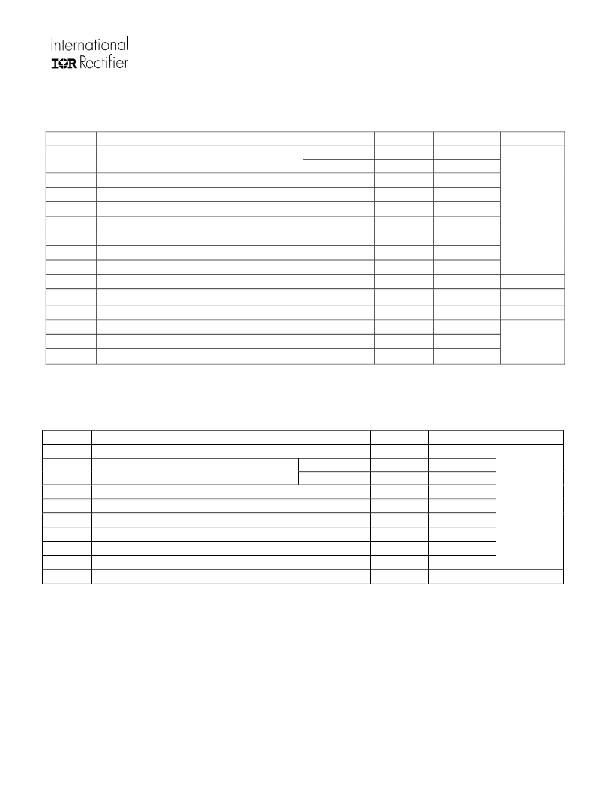
�Absolute� Maximum� Ratings�
�Absolute� Maximum� Ratings� indicate� sustained� limits� beyond� which� damage� to� the� device� may� occur.� All� voltage�
�parameters� are� absolute� voltages� referenced� to� COM.� The� thermal� resistance� and� power� dissipation� ratings� are�
�measured� under� board� mounted� and� still� air� conditions.�
�Symbol� Definition� Min.� Max.� Units�
�V� B�
�High-side� floating� supply� voltage�
�(AUIRS2110)� -0.3�
�(AUIRS2113)� -0.3�
�520� (?)�
�620� (?)�
�V� S�
�V� HO�
�High-side� floating� supply� offset� voltage� V� B� -� 20� V� B� +� 0.3�
�High-side� floating� output� voltage� V� S� -� 0.3� V� B� +� 0.3�
�V� CC�
�V� LO�
�Low-side� fixed� supply� voltage� -0.3� 20�
�Low-side� output� voltage� -0.3� V� CC� +� 0.3�
�V�
�V� DD�
�Logic� supply� voltage� -0.3�
�V� SS� +� 20� (?)�
�V� SS�
�V� IN�
�Logic� supply� offset� voltage� V� CC� -� 20� V� CC� +� 0.3�
�Logic� input� voltage� (HIN,� LIN� &� SD)� V� SS� -0.3� V� DD� +� 0.3�
�dV� S� /dt� Allowable� offset� supply� voltage� transient� (Fig.� 2)� —� 50�
�V/ns�
�P� D�
�Package� power� dissipation� @� TA� ≤� 25°C�
�—�
�1.25�
�W�
�Rth� JA�
�T� J�
�T� S�
�T� L�
�Thermal� resistance,� junction� to� ambient� —�
�Junction� temperature� —�
�Storage� temperature� -55�
�Lead� temperature� (soldering,� 10� seconds)� —�
�100�
�150�
�150�
�300�
�°C/W�
�°C�
�?� All� supplies� are� fully� tested� at� 25� V,� and� an� internal� 20� V� clamp� exists� for� each� supply.�
�Recommended� Operating� Conditions�
�The� input/output� logic� timing� diagram� is� shown� in� Figure� 1.� For� proper� operation� the� device� should� be� used� within�
�the� recommended� conditions.� The� V� S� and� V� SS� offset� rating� are� tested� with� all� supplies� biased at 15 V� differential.�
�Symbol�
�V� B�
�V� S�
�Definition�
�High-side� floating� supply� absolute� voltage�
�High-side� floating� supply� offset� voltage�
�Min.�
�V� S� +10�
�(AUIRS2110)� ?�
�(AUIRS2113)� ?�
�Max.�
�V� S� +20�
�500�
�600�
�Units�
�V� HO�
�High-side� floating� output� voltage� V� S�
�V� B�
�V� CC�
�V� LO�
�V� DD�
�Low-side� fixed� supply� voltage� 10�
�Low-side� output� voltage� 0�
�Logic� supply� voltage� V� SS� +� 3�
�20�
�V� CC�
�V� SS� +� 20�
�V�
�V� SS�
�Logic� ground� offset� voltage�
�-5� (??)�
�5�
�V� IN�
�Logic� input� voltage� (HIN,� LIN� &� SD)� V� SS�
�V� DD�
�T� A�
�Ambient� temperature� -40�
�125�
�°C�
�?�
�??�
�Logic� operational� for� V� S� of� -4� V� to� +500� V.� Logic� state� held� for� V� S� of� -4� V� to� –� V� BS.�
�(Please� refer� to� the� Design� Tip� DT97� -3� for� more� details).�
�When� V� DD� <� 5� V,� the� minimum� V� SS� offset� is� limited� to� –V� DD� .�
�www.irf.com�
�5�
�?� 2008� International� Rectifier�
�相关PDF资料 |
PDF描述 |
|---|---|
| ABM3-27.000MHZ-D2Y-T | CRYSTAL 27.000 MHZ 18PF SMD |
| ABM3-12.288MHZ-D2Y-T | CRYSTAL 12.288 MHZ 18PF SMD |
| RPM40-4815SGW | CONV DC/DC 40W 18-75VIN 15VOUT |
| RPM30-1215DE-DIN | CONV DC/DC 30W 9-18VIN +/-15VOUT |
| RPM30-1212DE-DIN | CONV DC/DC 30W 9-18VIN +/-12VOUT |
相关代理商/技术参数 |
参数描述 |
|---|---|
| AUIRS2112S | 功能描述:功率驱动器IC High Low 600V DRVR 10V 20V 290mA 140ns RoHS:否 制造商:Micrel 产品:MOSFET Gate Drivers 类型:Low Cost High or Low Side MOSFET Driver 上升时间: 下降时间: 电源电压-最大:30 V 电源电压-最小:2.75 V 电源电流: 最大功率耗散: 最大工作温度:+ 85 C 安装风格:SMD/SMT 封装 / 箱体:SOIC-8 封装:Tube |
| AUIRS2112STR | 功能描述:功率驱动器IC 600V High Low DRVR Automotive 290mA RoHS:否 制造商:Micrel 产品:MOSFET Gate Drivers 类型:Low Cost High or Low Side MOSFET Driver 上升时间: 下降时间: 电源电压-最大:30 V 电源电压-最小:2.75 V 电源电流: 最大功率耗散: 最大工作温度:+ 85 C 安装风格:SMD/SMT 封装 / 箱体:SOIC-8 封装:Tube |
| AUIRS2113S | 功能描述:功率驱动器IC HI LO SIDE DRVR 2-Ch 600V 140ns RoHS:否 制造商:Micrel 产品:MOSFET Gate Drivers 类型:Low Cost High or Low Side MOSFET Driver 上升时间: 下降时间: 电源电压-最大:30 V 电源电压-最小:2.75 V 电源电流: 最大功率耗散: 最大工作温度:+ 85 C 安装风格:SMD/SMT 封装 / 箱体:SOIC-8 封装:Tube |
| AUIRS2113STR | 功能描述:功率驱动器IC HI LO SIDE DRVR 2-Ch 600V 140ns RoHS:否 制造商:Micrel 产品:MOSFET Gate Drivers 类型:Low Cost High or Low Side MOSFET Driver 上升时间: 下降时间: 电源电压-最大:30 V 电源电压-最小:2.75 V 电源电流: 最大功率耗散: 最大工作温度:+ 85 C 安装风格:SMD/SMT 封装 / 箱体:SOIC-8 封装:Tube |
| AUIRS2117S | 功能描述:功率驱动器IC AUTO Grade Single Chnl 600V Driver RoHS:否 制造商:Micrel 产品:MOSFET Gate Drivers 类型:Low Cost High or Low Side MOSFET Driver 上升时间: 下降时间: 电源电压-最大:30 V 电源电压-最小:2.75 V 电源电流: 最大功率耗散: 最大工作温度:+ 85 C 安装风格:SMD/SMT 封装 / 箱体:SOIC-8 封装:Tube |
发布紧急采购,3分钟左右您将得到回复。