- 您现在的位置:买卖IC网 > PDF目录58231 > AVA-24+ (MINI-CIRCUITS) 5000 MHz - 20000 MHz RF/MICROWAVE WIDE BAND LOW POWER AMPLIFIER PDF资料下载
参数资料
| 型号: | AVA-24+ |
| 厂商: | MINI-CIRCUITS |
| 元件分类: | 放大器 |
| 英文描述: | 5000 MHz - 20000 MHz RF/MICROWAVE WIDE BAND LOW POWER AMPLIFIER |
| 封装: | 3 X 3 MM, ROHS COMPLIANT, PLASTIC, CASE DQ849, MCLP, SMT, QFN-8 |
| 文件页数: | 4/5页 |
| 文件大小: | 476K |
| 代理商: | AVA-24+ |
Wideband Monolithic PHEMT MMIC Amplifier
ISO 9001 ISO 14001 AS 9100 CERTIFIED
Mini-Circuits
P.O. Box 350166, Brooklyn, New York 11235-0003 (718) 934-4500 Fax (718) 332-4661 The Design Engineers Search Engine
Provides ACTUAL Data Instantly at
Notes: 1. Performance and quality attributes and conditions not expressly stated in this specification sheet are intended to be excluded and do not form a part of this specification sheet. 2. Electrical specifications
and performance data contained herein are based on Mini-Circuit’s applicable established test performance criteria and measurement instructions. 3. The parts covered by this specification sheet are subject to
Mini-Circuits standard limited warranty and terms and conditions (collectively, “Standard Terms”); Purchasers of this part are entitled to the rights and benefits contained therein. For a full statement of the Standard
Terms and the exclusive rights and remedies thereunder, please visit Mini-Circuits’ website at www.minicircuits.com/MCLStore/terms.jsp.
For detailed performance specs
& shopping online see web site
minicircuits.com
IF/RF MICROWAVE COMPONENTS
Page 4
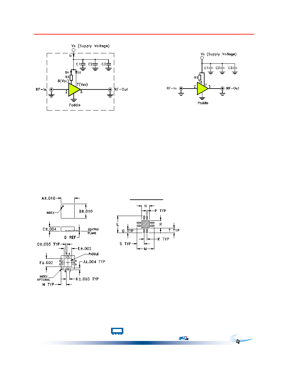
Characterization Test Circuit
AVA-24+
Fig 1.BlockDiagramofTestCircuitusedforcharacterization.(DUTsoldered
on Mini-Circuits Characterization Test Board TB-547-1+) Gain, Output power
at 1dB compression (P1dB), Noise Figure, Output IP3 (OIP3) are measured
using Agilent’s N5242A PNA-X microwave network analyzer.
Conditions:
1. Gain: Pin=-25 dBm
2. Output IP3 (OIP3): Two tones, spaced 1 MHz apart, -10 dBm/tone at output.
3. Vs adjusted for 5V at device (V
D1 and VD2), compensating loss of bias lines.
Recommended Application Circuit
(refer to evaluation board for PCB Layout and component values)
Fig 2. Recommended Application Circuit
Outline Drawing
Suggested Layout,
Tolerance to be within ±.002
PCB Land Pattern
A
B
C
D
E
FG
H
J
.118 .118 .035 .008 .067 .067 .012 .046 .016
3.00 3.00 0.89 0.20 1.70 1.70 0.30 1.17 0.41
K
L
M
NP
Q
RS
T
wt
.026 .148 .148 .067 .012 .031 .067 .061 .041 grams
0.66 3.76 3.76 1.70 0.30 0.79 1.70 1.55 1.04 0.02
Outline Dimensions (
)
inch
mm
C1=5.6pF
C2=18pF
C3=0.001F
R1=0 Ohm, size 0805 used for decoupling between
Vd1 & Vd2 to avoid oscillation. See “PL drawing”
TB-547-1+
相关PDF资料 |
PDF描述 |
|---|---|
| AVG4-00100400-14 | 100 MHz - 4000 MHz RF/MICROWAVE WIDE BAND LOW POWER AMPLIFIER |
| AWB7227RM52P8 | 2110 MHz - 2170 MHz RF/MICROWAVE NARROW BAND MEDIUM POWER AMPLIFIER |
| AWC6312RM9P9 | 1850 MHz - 1915 MHz RF/MICROWAVE NARROW BAND MEDIUM POWER AMPLIFIER |
| AWP-64107 | RF/MICROWAVE NARROW BAND MEDIUM POWER AMPLIFIER |
| AWP-64108 | RF/MICROWAVE NARROW BAND MEDIUM POWER AMPLIFIER |
相关代理商/技术参数 |
参数描述 |
|---|---|
| A-VA2510 | 制造商:DigitHead Inc 功能描述:Mono Audio Adapter - 3.5mm Plug to RCA Jack |
| AVA-3406-R3-01 | 制造商:Emerson Network Power 功能描述:AVANTELLIS 3406R3 PLATFORM CORE - Bulk |
| AVA-3406-R3-02 | 制造商:Emerson Network Power 功能描述:AVANTELLIS 3406R3 PLATFORM CORE DUAL BLADE - Bulk |
| AVA5-50 | 制造商:ANDREW MANUFACTURING 功能描述:AVA5-50 |
| AVA5-50FX | 制造商: 功能描述: 制造商:undefined 功能描述: |
发布紧急采购,3分钟左右您将得到回复。