- 您现在的位置:买卖IC网 > PDF目录295116 > AX500-1FG484I FPGA, 5376 CLBS, 286000 GATES, 763 MHz, PBGA484 PDF资料下载
参数资料
| 型号: | AX500-1FG484I |
| 元件分类: | FPGA |
| 英文描述: | FPGA, 5376 CLBS, 286000 GATES, 763 MHz, PBGA484 |
| 封装: | 1 MM PITCH, FBGA-484 |
| 文件页数: | 1/230页 |
| 文件大小: | 6485K |
| 代理商: | AX500-1FG484I |
当前第1页第2页第3页第4页第5页第6页第7页第8页第9页第10页第11页第12页第13页第14页第15页第16页第17页第18页第19页第20页第21页第22页第23页第24页第25页第26页第27页第28页第29页第30页第31页第32页第33页第34页第35页第36页第37页第38页第39页第40页第41页第42页第43页第44页第45页第46页第47页第48页第49页第50页第51页第52页第53页第54页第55页第56页第57页第58页第59页第60页第61页第62页第63页第64页第65页第66页第67页第68页第69页第70页第71页第72页第73页第74页第75页第76页第77页第78页第79页第80页第81页第82页第83页第84页第85页第86页第87页第88页第89页第90页第91页第92页第93页第94页第95页第96页第97页第98页第99页第100页第101页第102页第103页第104页第105页第106页第107页第108页第109页第110页第111页第112页第113页第114页第115页第116页第117页第118页第119页第120页第121页第122页第123页第124页第125页第126页第127页第128页第129页第130页第131页第132页第133页第134页第135页第136页第137页第138页第139页第140页第141页第142页第143页第144页第145页第146页第147页第148页第149页第150页第151页第152页第153页第154页第155页第156页第157页第158页第159页第160页第161页第162页第163页第164页第165页第166页第167页第168页第169页第170页第171页第172页第173页第174页第175页第176页第177页第178页第179页第180页第181页第182页第183页第184页第185页第186页第187页第188页第189页第190页第191页第192页第193页第194页第195页第196页第197页第198页第199页第200页第201页第202页第203页第204页第205页第206页第207页第208页第209页第210页第211页第212页第213页第214页第215页第216页第217页第218页第219页第220页第221页第222页第223页第224页第225页第226页第227页第228页第229页第230页
October 2009
i
2009 Actel Corporation
See the Actel website for the latest version of the datasheet.
v2.8
Axcelerator Family FPGAs
Leading-Edge Performance
350+ MHz System Performance
500+ MHz Internal Performance
High-Performance Embedded FIFOs
700 Mb/s LVDS Capable I/Os
Specifications
Up to 2 Million Equivalent System Gates
Up to 684 I/Os
Up to 10,752 Dedicated Flip-Flops
Up to 295 kbits Embedded SRAM/FIFO
Manufactured on Advanced 0.15
μm CMOS Antifuse
Process Technology, 7 Layers of Metal
Features
Single-Chip, Nonvolatile Solution
Up to 100% Resource Utilization with 100% Pin Locking
1.5V Core Voltage for Low Power
Footprint Compatible Packaging
Flexible, Multi-Standard I/Os:
–
1.5V, 1.8V, 2.5V, 3.3V Mixed Voltage Operation
–
Bank-Selectable I/Os – 8 Banks per Chip
–
Single-Ended I/O Standards: LVTTL, LVCMOS, 3.3V
PCI, and 3.3V PCI-X
–
Differential I/O Standards: LVPECL and LVDS
–
Voltage-Referenced I/O Standards: GTL+, HSTL
Class 1, SSTL2 Class 1 and 2, SSTL3 Class 1 and 2
–
Registered I/Os
–
Hot-Swap Compliant I/Os (except PCI)
–
Programmable Slew Rate and Drive Strength on
Outputs
–
Programmable Delay and Weak Pull-Up/Pull-Down
Circuits on Inputs
Embedded Memory:
–
Variable-Aspect 4,608-bit RAM Blocks (x1, x2, x4,
x9, x18, x36 Organizations Available)
–
Independent, Width-Configurable Read and Write Ports
–
Programmable Embedded FIFO Control Logic
Segmentable Clock Resources
Embedded Phase-Locked Loop:
–
14-200 MHz Input Range
–
Frequency Synthesis Capabilities up to 1 GHz
Deterministic, User-Controllable Timing
Unique In-System Diagnostic and Debug Capability
with Actel Silicon Explorer II
Boundary-Scan Testing Compliant with IEEE Standard
1149.1 (JTAG)
FuseLockTM
Secure
Programming
Technology
Prevents Reverse Engineering and Design Theft
e
u
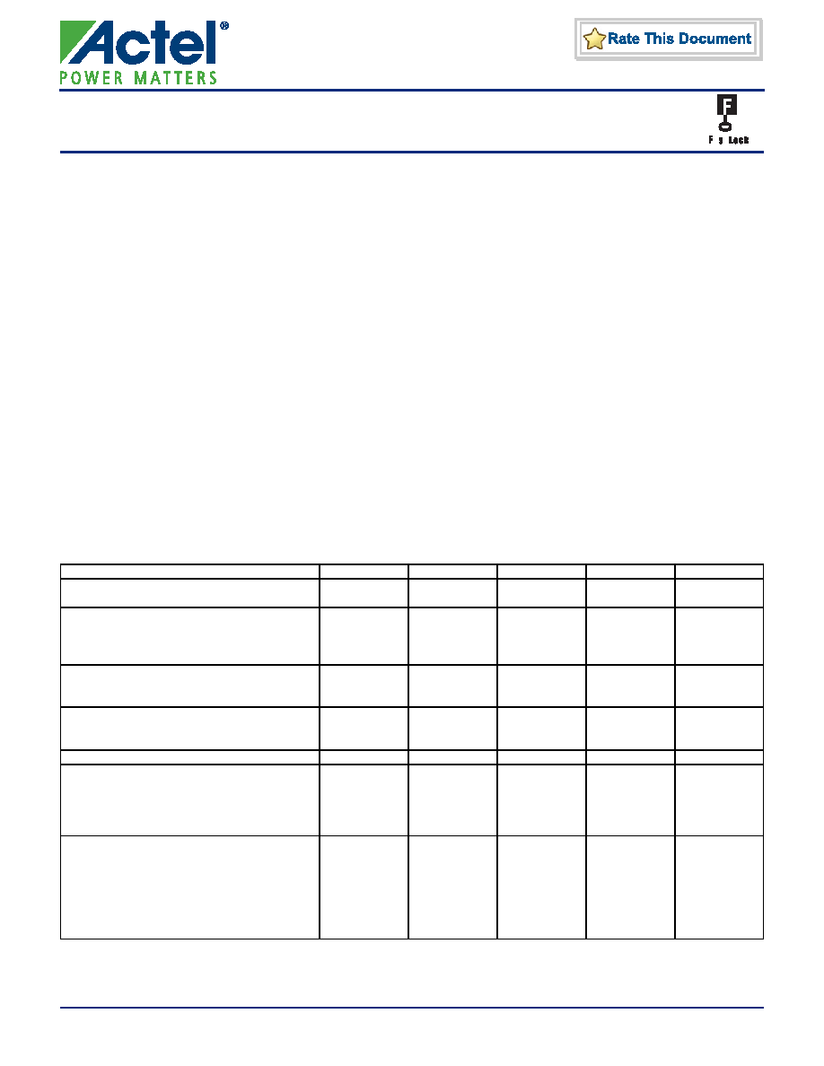
Table 1-1 Axcelerator Family Product Profile
Device
AX125
AX250
AX500
AX1000
AX2000
Capacity (in Equivalent System Gates)
125,000
250,000
500,000
1,000,000
2,000,000
Typical Gates
82,000
154,000
286,000
612,000
1,060,000
Modules
Register (R-cells)
672
1,408
2,688
6,048
10,752
Combinatorial (C-cells)
1,344
2,816
5,376
12,096
21,504
Maximum Flip-Flops
1,344
2,816
5,376
12,096
21,504
Embedded RAM/FIFO
Number of Core RAM Blocks
4
12
16
36
64
Total Bits of Core RAM
18,432
55,296
73,728
165,888
294,912
Clocks (Segmentable)
Hardwired
4
Routed
4
PLLs
8
888
8
I/Os
I/O Banks
8
Maximum User I/Os
168
248
336
516
684
Maximum LVDS Channels
84
124
168
258
342
Total I/O Registers
504
744
1,008
1,548
2,052
Package
CSP
PQFP
BGA
FBGA
CQFP
CCGA
180
256, 324
208
256, 484
208, 352
208
484, 676
208, 352
729
484, 676, 896
352
624
896, 1152
256, 352
624
v2.8
相关PDF资料 |
PDF描述 |
|---|---|
| AX500-1FG484MX79 | FPGA, 5376 CLBS, 286000 GATES, 763 MHz, PBGA484 |
| AX500-1FG484M | FPGA, 5376 CLBS, 286000 GATES, 763 MHz, PBGA484 |
| AX500-1FG484X79 | FPGA, 5376 CLBS, 286000 GATES, 763 MHz, PBGA484 |
| AX500-1FG484 | FPGA, 5376 CLBS, 286000 GATES, 763 MHz, PBGA484 |
| AX500-1FG676IX79 | FPGA, 5376 CLBS, 286000 GATES, 763 MHz, PBGA676 |
相关代理商/技术参数 |
参数描述 |
|---|---|
| AX500-1FG484M | 制造商:Microsemi Corporation 功能描述:FPGA Axcelerator Family 286K Gates 5376 Cells 763MHz 0.15um Technology 1.5V 484-Pin FBGA 制造商:Microsemi Corporation 功能描述:FPGA AXCELERATOR 286K GATES 5376 CELLS 763MHZ 0.15UM 1.5V 48 - Trays 制造商:Microsemi Corporation 功能描述:IC FPGA 317 I/O 484FBGA 制造商:Microsemi Corporation 功能描述:IC FPGA AXCELERATOR 500K 484FBGA |
| AX500-1FG676 | 功能描述:IC FPGA AXCELERATOR 500K 676FBGA RoHS:否 类别:集成电路 (IC) >> 嵌入式 - FPGA(现场可编程门阵列) 系列:Axcelerator 产品培训模块:Three Reasons to Use FPGA's in Industrial Designs Cyclone IV FPGA Family Overview 特色产品:Cyclone? IV FPGAs 标准包装:60 系列:CYCLONE® IV GX LAB/CLB数:9360 逻辑元件/单元数:149760 RAM 位总计:6635520 输入/输出数:270 门数:- 电源电压:1.16 V ~ 1.24 V 安装类型:表面贴装 工作温度:0°C ~ 85°C 封装/外壳:484-BGA 供应商设备封装:484-FBGA(23x23) |
| AX500-1FG676I | 功能描述:IC FPGA AXCELERATOR 500K 676FBGA RoHS:否 类别:集成电路 (IC) >> 嵌入式 - FPGA(现场可编程门阵列) 系列:Axcelerator 产品培训模块:Three Reasons to Use FPGA's in Industrial Designs Cyclone IV FPGA Family Overview 特色产品:Cyclone? IV FPGAs 标准包装:60 系列:CYCLONE® IV GX LAB/CLB数:9360 逻辑元件/单元数:149760 RAM 位总计:6635520 输入/输出数:270 门数:- 电源电压:1.16 V ~ 1.24 V 安装类型:表面贴装 工作温度:0°C ~ 85°C 封装/外壳:484-BGA 供应商设备封装:484-FBGA(23x23) |
| AX500-1FG676M | 制造商:Microsemi Corporation 功能描述:FPGA AXCELERATOR 286K GATES 5376 CELLS 763MHZ 0.15UM 1.5V 67 - Trays 制造商:Microsemi Corporation 功能描述:IC FPGA 336 I/O 676FBGA 制造商:Microsemi Corporation 功能描述:IC FPGA AXCELERATOR 500K 676FBGA |
| AX500-1FG896 | 制造商:ACTEL 制造商全称:Actel Corporation 功能描述:Axcelerator Family FPGAs |
发布紧急采购,3分钟左右您将得到回复。