- 您现在的位置:买卖IC网 > Datasheet目录39 > BD3504FVM-TR (Rohm Semiconductor)IC REG CTRLR SGL POS ADJ 8MSOP Datasheet资料下载
参数资料
| 型号: | BD3504FVM-TR |
| 厂商: | Rohm Semiconductor |
| 文件页数: | 10/19页 |
| 文件大小: | 605K |
| 描述: | IC REG CTRLR SGL POS ADJ 8MSOP |
| 标准包装: | 2,000 |
| 类型: | 正,可调式 |
| 输出数: | 1 |
| 输出电压: | 0.65 V ~ 2.5 V |
| 输入电压: | 4.5 V ~ 5.5 V |
| 工作温度: | -10°C ~ 100°C |
| 封装/外壳: | 8-VSSOP,8-MSOP(0.118",3.00mm 宽) |
| 供应商设备封装: | 8-MSOP |
| 包装: | 带卷 (TR) |
BD3504FVM,BD3500FVM,BD3501FVM,BD3502FVM
Technical Note
10/16
www.rohm.com
2010.05 - Rev.A
?2010 ROHM Co., Ltd. All rights reserved.
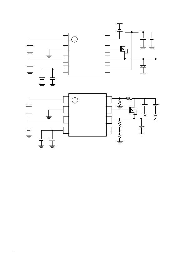
?SPAN class="pst BD3504FVM-TR_2649171_6">Application circuit
C3
C2
Ven
C4
C5
VIN
C1
Vcc
+
1
2
3
4
8
7
6
5
VIN
R1
R2
C3
Ven
C4
C1
Vcc
+
1
2
3
4
8
7
6
5
C2
R1
R2
?SPAN class="pst BD3504FVM-TR_2649171_6">Directions for pattern layout of PCB
鸅ecause a VIN input capacitor causes impedance to drop, mount it as close to the VIN terminal as possible and use thick
wiring patterns. In the event that it causes the wire to come in contact with the inner-layer ground plane, use a plurality of
through holes.
鸅ecause the NRCS terminal is analog I/O, take care to noise. In particular, high-frequency noise of GND may cause IC
maloperation through capacitors. It is recommended to connect GND of NRCS capacitor to IC GND terminal at one
point.
鸗he VFB terminal is an output voltage sense line. Effects of wiring impedance can be ignored by sensing the output
voltage from the load side, but increased sense wiring causes VFB to be susceptible to noise, to which care must be
taken.
鸅ecause the GND terminal is GND to be used in analog circuit inside BD3501/02/04FVM, connect it at one point to
inner-layer GND of substrate by as short pattern as possible. Arrange a bypass capacitor across VCC and GND as close
as possible so that a loop can be minimized.
鸗he G terminal is a terminal for gate drive. If long wiring is inevitable, increase the pattern width and lower impedance.
鸋eat generated in the output transistor can be calculated by:
(VIN - VOUT) ?Io(Max)
Design heat generation not to exceed the guarantee temperature of transistor.
鸆onnect the output capacitor with thick short wiring so that the impedance is lowered. Connect capacitor GND to
inner-layer GND plane by a plurality of through holes.
相关PDF资料 |
PDF描述 |
|---|---|
| BD3521FVM-TR | IC REG CTRLR SGL 1.5V MSOP8 |
| BD9153MUV-E2 | IC REG TRPL BCK/LINEAR 24VQFN |
| CAT2300VP2-GT3 | IC SENSE FET CONTROLLER 8TDFN |
| CAT34TS02VP2GT4A | IC TEMP SENSOR 2K MEMORY 8TDFN |
| CAT6095VP2-GT4 | IC TEMP SENSOR STAND ALONE 8TDFN |
相关代理商/技术参数 |
参数描述 |
|---|---|
| BD3505 | 制造商:WTE 制造商全称:Won-Top Electronics 功能描述:35A BOSCH TYPE PRESS-FIT DIODE |
| BD3506 | 制造商:WTE 制造商全称:Won-Top Electronics 功能描述:35A BOSCH TYPE PRESS-FIT DIODE |
| BD3506EFV | 制造商:ROHM 制造商全称:Rohm 功能描述:Nch FET Ultra LDO for PC Chipsets |
| BD3506F | 制造商:ROHM 制造商全称:Rohm 功能描述:Nch FET Ultra LDO for PC Chipsets |
| BD3506F_08 | 制造商:ROHM 制造商全称:Rohm 功能描述:Ultra Low Dropout Linear Regulators for PC Chipsets |
发布紧急采购,3分钟左右您将得到回复。