- 您现在的位置:买卖IC网 > PDF目录227782 > BD5244G 1-CHANNEL POWER SUPPLY SUPPORT CKT, PDSO5 PDF资料下载
参数资料
| 型号: | BD5244G |
| 元件分类: | 电源管理 |
| 英文描述: | 1-CHANNEL POWER SUPPLY SUPPORT CKT, PDSO5 |
| 封装: | ROHS COMPLIANT, SSOP-5 |
| 文件页数: | 6/10页 |
| 文件大小: | 269K |
| 代理商: | BD5244G |
Technical Note
5/9
BD52
□□G, BD52□□FVE, BD53□□G, BD53□□FVE series
www.rohm.com
2009.06 - Rev.B
2009 ROHM Co., Ltd. All rights reserved.
Setting of Detector Delay Time
This detector IC can be set delay time at the rise of VDD by the capacitor connected to CT terminal.
Delay time at the rise of VDD TPLH:Time until when Vout rise to 1/2 of VDD after VDD rise up and beyond the release
voltage(VDET+VDET)
TPLH = -CCT×RCT×ln
CCT:
CT pin Externally Attached Capacitance
RCT : CT pin Internal Impedance (P.2 RCT refer.)
VCTH:
CT pin Threshold Voltage(P.2 VCTH refer.)
Ln : Natural Logarithm
Reference Data of Falling Time (TPHL) Output
Examples of Falling Time (TPHL) Output
Part Number
tPHL[s] -40°C
tPHL[s] ,+25°C
tPHL[s],+105°C
BD5227G
30.8
30
28.8
BD5327G
26.8
26
24.8
*This data is for reference only.
The figures will vary with the application, so please confirm actual operating conditions before use.
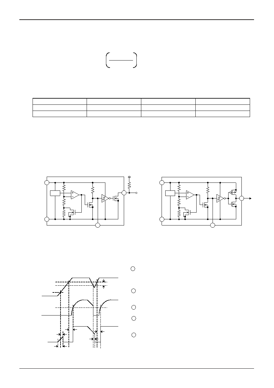
Explanation of Operation
For both the open drain type (Fig.15) and the CMOS output type (Fig.16), the detection and release voltages are used as
threshold voltages. When the voltage applied to the VDD pins reaches the applicable threshold voltage, the VOUT terminal
voltage switches from either “High” to “Low” or from “Low” to “High”. Because the BD52
□□G/FVE series uses an open drain
output type, it is possible to connect a pull-up resistor to VDD or another power supply [The output “High” voltage (VOUT) in
this case becomes VDD or the voltage of the other power supply].
Fig.15 (BD52
□□Type Internal Block Diagram)
Fig.16 (BD53
□□Type Internal Block Diagram)
Timing Waveforms
Example: the following shows the relationship between the input voltage VDD, the CT Terminal Voltage VCT and the output
voltage VOUT when the input power supply voltage VDD is made to sweep up and sweep down (The circuits are those in
Fig.15 and 16).
1
When the power supply is turned on, the output is unsettled from
after over the operating limit voltage (VOPL) until TPHL. There fore it is
possible that the reset signal is not outputted when the rise time of
VDD is faster than TPHL.
2
When VDD is greater than VOPL but less than the reset release
voltage (VDET+
VDET), the CT terminal (VCT) and output (VOUT)
voltages will switch to L.
3
If VDD exceeds the reset release voltage (VDET+
VDET), then
VOUT switches from L to H (with a delay to the CT terminal).
4
If VDD drops below the detection voltage (VDET) when the power
supply is powered down or when there is a power supply fluctuation,
VOUT switches to L (with a delay of TPHL).
5
The potential difference between the detection voltage and the
release voltage is known as the hysteresis width (
VDET). The
system is designed such that the output does not flip-flop with power
supply
fluctuations
within
this
hysteresis
width,
preventing
malfunctions due to noise.
Vref
VDD
GND
CT
R1
R2
R3
Q3
Q1
VOUT
RESET
RL
VDD
Vref
VDD
GND
CT
R1
R2
R3
Q3
Q2
VOUT
RESET
Q1
VDD
VDD
VDET+ΔVDET
VDET
VOPL
0V
1/2 VDD
TPHL
①
TPLH
TPHL
TPLH
②
③
④
VCT
⑤
VOUT
Fig.17
VDD-VCTH
VDD
相关PDF资料 |
PDF描述 |
|---|---|
| BU4341G-TR | 1-CHANNEL POWER SUPPLY SUPPORT CKT, PDSO5 |
| BP2320-7RVW | 2-OUTPUT 180 W DC-DC REG PWR SUPPLY MODULE |
| BP2320-9GTI | 2-OUTPUT 180 W DC-DC REG PWR SUPPLY MODULE |
| BU4941F | 1-CHANNEL POWER SUPPLY SUPPORT CKT, PDSO4 |
| BP2320-9DG | 2-OUTPUT 180 W DC-DC REG PWR SUPPLY MODULE |
相关代理商/技术参数 |
参数描述 |
|---|---|
| BD5244G/FVE | 制造商:未知厂家 制造商全称:未知厂家 功能描述:VOLTAGE DETECTOR IC with adjustable delay time |
| BD5244G-TR | 功能描述:电压监测器/监控器 CMOS DETEC VOLT 4.4V RoHS:否 制造商:Texas Instruments 监测电压数:2 监测电压:Adjustable 输出类型:Open Drain 欠电压阈值: 过电压阈值: 准确性:1 % 工作电源电压:1.5 V to 6.5 V 工作电源电流:1.8 uA 最大工作温度:+ 125 C 封装 / 箱体:SON-6 安装风格:SMD/SMT |
| BD5245 | 制造商:未知厂家 制造商全称:未知厂家 功能描述:VOLTAGE DETECTOR IC with adjustable delay time |
| BD5245FVE | 制造商:ROHM 制造商全称:Rohm 功能描述:Voltage Detector IC with Adjustable Output Delay |
| BD5245FVETR | 制造商:ROHM Semiconductor 功能描述: |
发布紧急采购,3分钟左右您将得到回复。