- 您现在的位置:买卖IC网 > Datasheet目录316 > BD9206EFV-E2 (Rohm Semiconductor)IC LED DRIVER 6V LCD 20HTSSOP Datasheet资料下载
参数资料
| 型号: | BD9206EFV-E2 |
| 厂商: | Rohm Semiconductor |
| 文件页数: | 13/18页 |
| 文件大小: | 0K |
| 描述: | IC LED DRIVER 6V LCD 20HTSSOP |
| 标准包装: | 1 |
| 恒定电流: | 是 |
| 恒定电压: | 是 |
| 拓扑: | PWM |
| 输出数: | 6 |
| 内部驱动器: | 无 |
| 类型 - 主要: | 背光 |
| 类型 - 次要: | 白色 LED |
| 电源电压: | 8 V ~ 30 V |
| 输出电压: | 5V |
| 安装类型: | 表面贴装 |
| 封装/外壳: | 20-VSSOP(0.173",4.40mm 宽) |
| 供应商设备封装: | 20-HTSSOP |
| 包装: | 标准包装 |
| 工作温度: | -40°C ~ 85°C |
| 其它名称: | BD9206EFV-E2DKR |
�� �
�
�BD9206EFV�
�Datasheet�
�●� Operational� Notes�
�1.)� T� he� absolute� maximum� ratings�
�We� pay� sufficient� attention� for� quality� control� to� this� product� but� If� the� absolute� maximum� ratings� are� exceeded,� such� as� with�
�applied� voltage� or� operational� temperature� range,� a� degradation� or� a� destruction� may� occur.� The� short� or� open� modes� cannot� be�
�specified.� so� if� special� modes� which� exceed� the� absolute� maximum� ratings� are� assumed,� physical� safety� precautions� such� as� fuses�
�should� be� in� place.�
�2.)� Reverse� connection� of� power� supply� connector�
�The� reverse� connection� of� power� connector� may� cause� damage� to� IC.� Please� take� countermeasures� such� as� inserting� a�
�diode� between� the� power� supply� and� IC’s� external� power� supply� pin� for� protection� against� the� damage� caused� by� the�
�reverse� connection.�
�3.)� Power� supply� line�
�The� return� of� the� regenerated� current� is� caused� by� the� back� electromotive� force� of� the� external� coil,� so� please� take� the�
�measures� such� as� inserting� a� capacitor� between� power� supply� and� GND� as� a� route� of� regenerated� current,� and� determine�
�the� capacitance� value� after� thoroughly� ensuring� that� there� is� no� problems� in� the� Characteristics� of� electrolyte� capacitor,�
�such� as� no� loss� of� capacitance� at� low� temperature.� Heat� design� should� take� into� account� of� power� dissipation� (Pd)� under� actual�
�usage� conditions,� with� wide� enough� margins�
�4.)� GND� Potential�
�The� potential� of� the� GND� terminal� should� be� the� minimum� potential� under� all� operating� conditions.�
�5.)� Heat� Design�
�Heat� design� should� take� into� account� of� power� dissipation� under� actual� usage� conditions,� with� wide� enough� margins.�
�6.)� Short-circuiting� between� Terminals� and� Incorrect� Mounting�
�When� mounting� to� the� PWB,� pay� special� attention� to� the� direction� and� proper� placement� of� the� IC.� If� the� IC� is� attached� incorrectly,�
�it� may� be� destroyed.� Furthermore,� there� is� also� a� possibility� of� breakdown,� w� hen� the� foreign� body� enters� during� outputting� and�
�between� power� supply� and� GND.�
�7.)� The� operation� in� the� strong� magnetic� fields�
�Please� be� careful� that� there� is� a� possibility� of� malfunction� which� is� happening� when� you� use� it� in� a� strong� electromagnetic�
�field.�
�8.)� ASO�
�Please� do� the� setting� in� such� a� way� that� the� output� Tr� does� not� exceed� the� absolute� maximum� rating� and� ASO� in� case� of�
�using� this� IC.� For� CMOS� IC� and� the� IC� with� more� than� one� power� supply,� a� rush� current� may� flow� instantaneously� at� the�
�time� of� power� on,� so� please� be� careful� about� power� supply� coupling� capacitance,� power� supply,� GND� pattern� wiring� width�
�and� length.�
�9.)� Thermal� shutdown� circuit� (TSD� circuit)�
�This� IC� incorporates� a� built-in� thermal� shutdown� circuit� (TSD� circuit).� The� TSD� circuit� is� that� has� designed� only� to� shut� the�
�IC� off� to� prevent� the� thermal� runaway� operation� ,� not� for� IC� protection� or� guarantee� as� purpose.� Therefore,� please� do� not�
�continue� to� use� the� IC� after� operating� this� circuit� and� also� do� not� use� the� IC� designating� operation� as� prerequisite.�
�10.)� Inspection� of� the� Set� Substrate�
�If� a� condenser� is� connected� to� a� pin� with� low� impedance� when� inspecting� the� set� substrate,� stress� may� be� placed� on� the� IC,�
�so� please� be� sure� to� discharge� after� each� process.� Moreover,� please� be� sure� to� turn� off� the� power� supply� before� connecting�
�&� inspecting� or� before� detaching� when� it� is� connected� to� jig� at� inspection� process.�
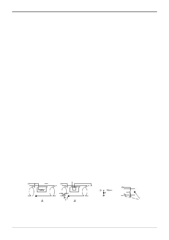
�11.)� About� IC� terminal� input�
�This� IC� is� a� monolithic� IC,� and� there� are� a� P+� isolation� and� the� P� substrate� for� separation� of� element� between� each� element.� There� is�
�a� P-N� junction� formed� between� this� P-layer� and� each� element’s� N-layer,� forming� every� p� arasitic� element,� as� shown� in� Fig.15,� when�
�resistance� and� transistor� are� connected� with� terminal�
�〇� In� the� case� of� GND>� (� terminal� A� )� with� resistance� or� GND>(terminal� B)� with� transistor(NPN),� the� P-N� junction� operates� as� a�
�parasitic� diode.�
�〇� In� addition,� when� GND>� (terminal� B)� with� the� transistor� (NPN),� the� parasitic� NPN� transistor� operates� due� to� the� aforementioned�
�parasitic� diode� and� the� N� layer� of� the� other� element� approached�
�With� the� IC’s� configuration,� the� production� of� parasitic� elements� is� inevitable.� The� operation� of� parasitic� elements� causes�
�interferences� between� circuits,� leading� to� malfunction� and� even� destruction.� Therefore,� uses� which� cause� the� parasitic� elements�
�to� operate,� such� as� applying� voltage� to� the� input� terminal� which� is� lower� than� the� GND� (P-substrate),� should� be� avoided.�
�抵抗�
�(端子B)�
�(terminalA)�
�(端子A)�
�P� +�
�N�
�Resistance�
�P�
�N�
�P� +�
�N�
�(terminalB)�
�C�
�P� +�
�N�
�Transistor�
�トランジスタ�
�B�
�(NPN)�
�N�
�P�
�N�
�E�
�P� +�
�N�
�GND�
�(terminalA)�
�(端子A)�
�寄生� 素子�
�Parasitic� Element�
�(terminalB)�
�(端子B)�
�B� C�
�E�
�寄生素子�
�P� 基板�
�寄生素子�
�P� Substrate� Parasitic� Element�
�P� Substrate�
�P� 基板�
�GND�
�近接� approached�
�other� element� する他の素子�
�GND�
�Parasitic� Element�
�GND�
�生素子�
�Parasitic� 寄� Element�
�GND�
�22� バイ� ポ� ーラ� IC� of� bipolar� IC�
�Figure� Fig..11� Simple� Structure� の簡� 易構造例� (Sample)�
�Status� of� this� document�
�The� Japanese� version� of� this� document� is� formal� specification.� A� customer� may� use� this� translation� version�
�only� for� a� reference� to� help� reading� the� formal� version.�
�If� there� are� any� differences� in� translation� version� of� this� document� formal� version� takes� priority.�
�www.rohm.com�
�?� 2012� ROHM� Co.,� Ltd.� All� rights� reserved.�
�TSZ22111� ?� 15� ?� 001�
�13/15�
�TSZ02201-0F1F0C100070-1-2�
�20.Sep.2012� Rev.001�
�相关PDF资料 |
PDF描述 |
|---|---|
| BD9207FPS-E2 | IC LED DVR STEPDWN 1.5A TO252S-5 |
| BH-14E_TI-20T_CTI | ADAPTER PIN CONVERTER 14-20 PIN |
| BH-20E_CTI-60T_TI | ADAPTER PIN CONVERTER 20-60 PIN |
| BH-ADP-ISO20 | ISOLATION ADAPTER 20-PIN TI JTAG |
| BH-GANG2000 | GANG2000 PROGRAMMER TI 32BIT MCU |
相关代理商/技术参数 |
参数描述 |
|---|---|
| BD9207FPS | 制造商:ROHM 制造商全称:Rohm 功能描述:Step-down type with 1.5A output |
| BD9207FPS-E2 | 功能描述:IC LED DVR STEPDWN 1.5A TO252S-5 RoHS:是 类别:集成电路 (IC) >> PMIC - LED 驱动器 系列:- 标准包装:60 系列:- 恒定电流:- 恒定电压:- 拓扑:线性(LDO),PWM,升压(升压) 输出数:8 内部驱动器:是 类型 - 主要:背光 类型 - 次要:RGB,白色 LED 频率:500kHz ~ 1.5MHz 电源电压:4.75 V ~ 26 V 输出电压:45V 安装类型:* 封装/外壳:* 供应商设备封装:* 包装:* 工作温度:-40°C ~ 85°C |
| BD92111F-GE2 | 功能描述:PFC DIRECT CURRENT RESONANCE TYP 制造商:rohm semiconductor 系列:* 包装:剪切带(CT) 零件状态:在售 安装类型:表面贴装 封装/外壳:18-SOIC(0.213",5.40mm 宽) 供应商器件封装:18-SOP 标准包装:1 |
| BD9211F | 制造商:ROHM 制造商全称:Rohm 功能描述:Silicon Monolithic Integrated Circuit |
| BD9215AFV | 制造商:ROHM 制造商全称:Rohm 功能描述:Silicon Monolithic Integrated Circuit |
发布紧急采购,3分钟左右您将得到回复。