参数资料
| 型号: | BG2B-5015 |
| 厂商: | Powerex Inc |
| 文件页数: | 4/5页 |
| 文件大小: | 0K |
| 描述: | KIT DEV BOARD 2CN 5A FOR IGBT |
| 标准包装: | 2 |
| 主要目的: | 电源管理,IGBT 电源模块驱动器 |
| 嵌入式: | 否 |
| 已用 IC / 零件: | Powerex IGBT 模块 |
| 已供物品: | 5 个板 |
| 相关产品: | MG800J2YS50A-ND - IGBT MOD CMPCT 600V 800A MG600Q2YS60A-ND - IGBT MOD CMPCT 1200V 600A MG600J2YS61A-ND - IGBT MOD CMPCT DUAL 600V 600A MG400V2YS60A-ND - IGBT MOD CMPCT DUAL 1700V 400A MG400Q2YS60A-ND - IGBT MOD CMPCT DUAL 1200V 400A MG400J2YS61A-ND - IGBT MOD CMPCT DUAL 600V 400A MG300Q2YS60A-ND - IGBT MOD CMPCT DUAL 1200V 300A MG200Q2YS60A-ND - IGBT MOD CMPCT DUAL 1200V 200A CP30TD1-12A-ND - DIP-CIB MOD 600V 30A CP25TD1-24A-ND - DIP-CIB MOD 1200V 25A 更多... |
�� �
�
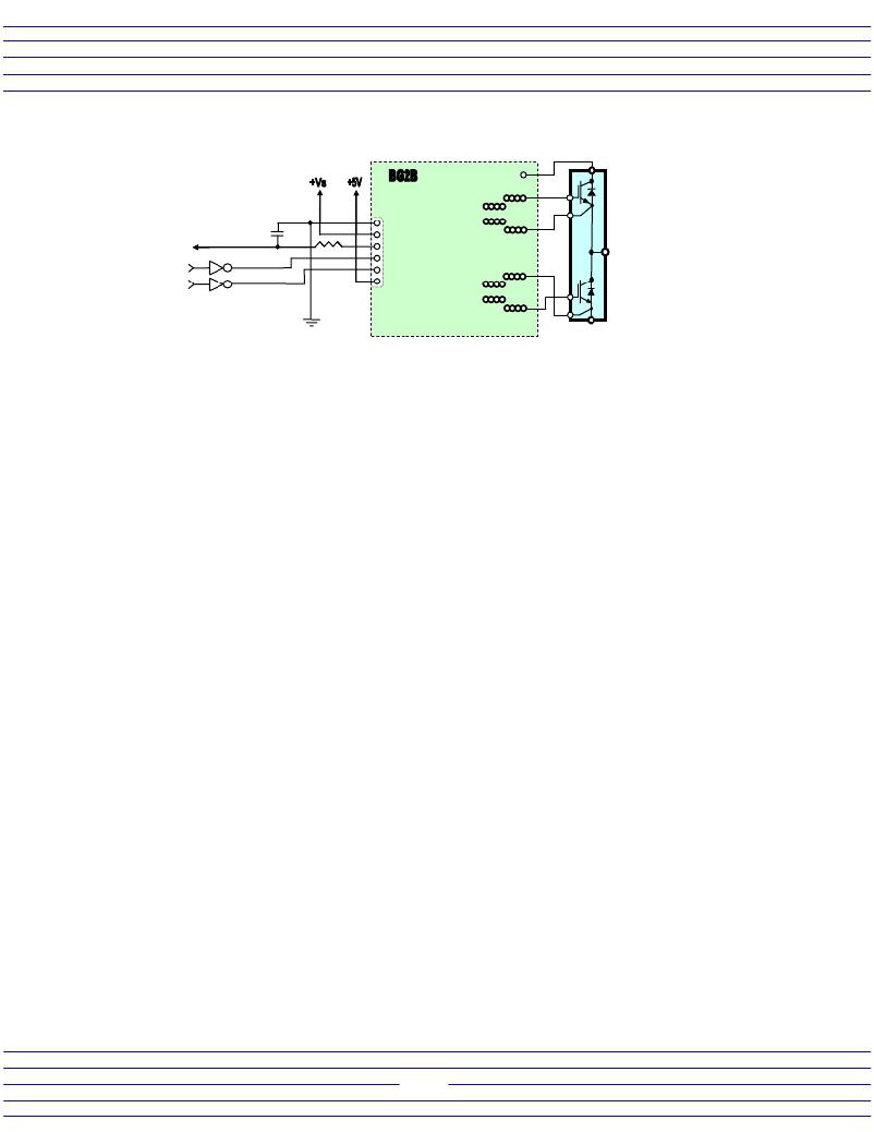
�Figure� 4:� BG2B� External� Wiring� Diagram�
�C1�
�CN2�
�RC� Filter� to�
�remove� noise� on�
�fault� signal�
�RC~10us�
�CN1�
�GND�
�+V� S�
�G1�
�E1�
�To� logic�
�level� control�
�circuits�
�CMOS� type�
�1�
�FO�
�IN1�
�IN2�
�+V� L�
�E2�
�G2�
�C2E1�
�buffer� must� sink�
�15mA�
�E2�
�IGBT� Module�
�Interface� Circuit� Requirements:� A� typical� interface� circuit� for� the� BG2B� is� shown� in� Figure� 4.� A� single� control�
�power� supply� (+V� S� )� is� connected� to� pin� 5� of� CN1� with� its� common� at� pin� 6.� This� supply� provides� all� of� the� gate�
�drive� power� for� both� channels� via� the� hybrid� DC� to� DC� converters.� The� current� drawn� from� the� +V� S� supply� will�
�vary� from� less� than� 100mA� to� more� than� 500mA� depending� on� the� switching� frequency� and� size� of� IGBT� being�
�driven.� Consult� the� hybrid� gate� driver� application� notes� for� details� on� determining� the� required� supply� current� for�
�the� gate� driver.� The� gate� driver� supply� current� can� then� be� converted� into� current� drawn� from� the� +V� S� supply�
�using� the� efficiency� specification� on� the� DC� to� DC� converter� data� sheet.�
�A� 5V� logic� supply� is� connected� at� pin� 1� of� CN1� and� shares� the� same� common� at� pin� 6� of� CN1� as� the�
�15V� control� supply.� The� 5V� supply� is� directly� connected� to� pin� 14� of� the� hybrid� gate� driver� which� is� internally�
�connected� to� the� anode� of� the� LED� in� the� high� speed� opto� coupler.� The� 5V� supply� is� also� used� to� pull� the� output�
�side� of� the� fault� isolation� opto� couplers� high.�
�The� control� signal� interface� is� designed� for� use� with� standard� 5V� CMOS� logic.� The� control� input� signals� at�
�pins� 2� and� 3� of� connector� CN1� are� used� to� turn� the� IGBTs� on� and� off.� These� signals� are� active� low� which� means�
�that� the� gate� driver� output� will� be� high� (IGBT� on)� when� they� are� pulled� low.� These� control� pins� are� connected�
�directly� to� pin� 13� of� the� hybrid� gate� driver� which� is� connected� internally� through� a� 180� Ω� limiting� resistor� to� the�
�cathode� of� the� LED� in� the� high� speed� opto� coupler� (see� figure� 1).� When� the� control� signal� is� pulled� low,� current�
�flows� from� the� 5V� logic� supply� through� the� LED� to� turn� the� gate� driver’s� output� on.� The� control� pins� must� be�
�pulled� low� with� a� buffer� that� is� capable� of� sinking� at� least� 16mA� in� order� to� turn� on� the� high� speed� opto� coupler�
�inside� the� hybrid� gate� driver.� A� CMOS� buffer� that� actively� pulls� its� output� high� in� the� off� state� (74HC04� or� similar)�
�is� recommended� for� maintaining� good� common� mode� noise� immunity.� Open� collector� drive� that� allows� IN1� and�
�IN2� to� float� will� degrade� common� mode� noise� immunity� and� is� therefore� not� recommended.�
�The� fault� signal� line� on� pin� 4� of� CN1� is� active� low� which� means� that� a� fault� condition� will� be� indicated� by�
�a� low� level� signal.� During� normal� operation� pin� 4� is� pulled� high� to� the� +V� L� supply� by� the� 4.7K� resistor� R3.� If�
�either� of� the� hybrid� gate� drivers� detects� a� short� circuit� condition� its� fault� isolation� opto� (OP1,� OP2)� will� turn� on�
�and� pull� pin� 4� of� CN1� low.� When� a� fault� is� detected� the� hybrid� gate� drivers� disable� the� output� and� produce� a�
�fault� signal� for� a� minimum� of� 1ms.� Any� signal� on� the� fault� line� that� is� significantly� shorter� than� 1ms� can� not� be� a�
�legitimate� fault� so� it� should� be� ignored.� Therefore,� for� a� robust� noise� immune� design,� it� is� recommended� that� an�
�RC� filter� with� a� time� constant� of� approximately� 10� μ� s� be� added� between� pin� 4� and� the� controller� as� shown� in�
�figure� 4.�
�Printed� Circuit� Layout:� Figure� 5� shows� the� layout� of� the� BG2B� two� channel� gate� driver� board.� The� compact� 3� ”�
�x� 2.2� ”� circuit� board� with� only� 24� components� clearly� demonstrates� the� advantage� of� using� hybrid� gate� drivers�
�and� DC� to� DC� converters.� One� important� feature� is� the� use� of� three� ground� plane� islands� for� the� regions� of� the�
�PCB� having� high� voltage� differences.� Two� of� the� islands� are� tied� to� the� IGBT� emitter/circuit� common� (Pin� 2� of�
�the� DC� to� DC� converters)� of� each� output� channel.� The� third� island� is� connected� to� logic� interface� common� at� pin�
�6� of� CN1.� This� layout� provides� shielding� to� help� prevent� undesirable� coupling� of� noise� between� the� control� side�
�and� the� gate� drive� channels.�
�Additional� Information:� Detailed� information� about� the� operation� and� electrical� characteristics� of� the� M57159L-�
�01,� VLA503-01� and� VLA-504-01� hybrid� gate� drivers� can� be� found� on� the� individual� device� data� sheets.� Electrical�
�4�
�相关PDF资料 |
PDF描述 |
|---|---|
| BG2C-5015 | KIT DEV BOARD 5A FOR IGBT |
| BH-0111 | FUSEBLOCK 1 HOLE #1 STUD SIZE |
| BJ150 | TRS BLKHD PUSH-ON JACK STR SLD |
| BJ157F-2C | TRS BULKHD JACK STR FLNG SLD POT |
| BJ157 | TRS BLKHD JACK STR FRONT MT SLD |
相关代理商/技术参数 |
参数描述 |
|---|---|
| BG2B-F | 制造商:Powerex Power Semiconductors 功能描述:KIT DEVELOPMENT ACCY GATE DVR 制造商:Powerex Power Semiconductors 功能描述:DEV KIT, M57145L-01, M57160AL-01, WITH BARE PCB; Silicon Manufacturer:Powerex; Silicon Core Number:BG1A-KA; Kit Application Type:Driver - Transistor; Application Sub Type:IGBT Gate Driver; Leaded Process Compatible:No ;RoHS Compliant: No 制造商:Powerex Power Semiconductors 功能描述:GATE DRIVER |
| BG2C | 制造商:Powerex Power Semiconductors 功能描述:GATE DRIVER |
| BG2C-3015 | 功能描述:KIT DEV BOARD 3A FOR IGBT RoHS:否 类别:编程器,开发系统 >> 评估演示板和套件 系列:- 标准包装:1 系列:PCI Express® (PCIe) 主要目的:接口,收发器,PCI Express 嵌入式:- 已用 IC / 零件:DS80PCI800 主要属性:- 次要属性:- 已供物品:板 |
| BG2C-5015 | 功能描述:KIT DEV BOARD 5A FOR IGBT RoHS:否 类别:编程器,开发系统 >> 评估演示板和套件 系列:- 标准包装:1 系列:PCI Express® (PCIe) 主要目的:接口,收发器,PCI Express 嵌入式:- 已用 IC / 零件:DS80PCI800 主要属性:- 次要属性:- 已供物品:板 |
| BG2D | 功能描述:KIT DESIGN FOR NX SERIES IGBT RoHS:是 类别:编程器,开发系统 >> 评估板 - DC/DC 与 AC/DC(离线)SMPS 系列:NX 产品培训模块:Obsolescence Mitigation Program 标准包装:1 系列:True Shutdown™ 主要目的:DC/DC,步升 输出及类型:1,非隔离 功率 - 输出:- 输出电压:- 电流 - 输出:1A 输入电压:2.5 V ~ 5.5 V 稳压器拓扑结构:升压 频率 - 开关:3MHz 板类型:完全填充 已供物品:板 已用 IC / 零件:MAX8969 |
发布紧急采购,3分钟左右您将得到回复。