- 您现在的位置:买卖IC网 > PDF目录295140 > BH31FB1WG-TR FIXED POSITIVE REGULATOR, PDSO5 PDF资料下载
参数资料
| 型号: | BH31FB1WG-TR |
| 元件分类: | 固定正电压单路输出标准稳压器 |
| 英文描述: | FIXED POSITIVE REGULATOR, PDSO5 |
| 封装: | SSOP-5 |
| 文件页数: | 7/9页 |
| 文件大小: | 850K |
| 代理商: | BH31FB1WG-TR |
7/8
Noise terminal (BH
MA3WHFV)
The terminal is directly connected to inward normal voltage source. Because this has low current ability, load exceeding
100nA will cause some instability at the output. For such reasons, we urge you to use ceramic capacitors which have less
leak current. When choosing noise the current reduction capacitor, there is a trade-off between boot-up time and stability. A
bigger capacitor value will result in lesser oscillation but longer boot-up time for VOUT.
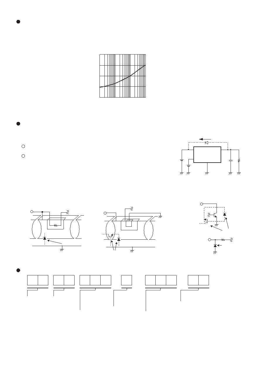
Fig. 35: VOUT startup time vs. noise-filtering capacitor capacitance characteristics (Example)
~ Condition ~
VIN=4.0V
Cin=1.0F
Co=1.0F
ROUT=3.0k
Ta=25
BH30MA3WHFV
100
10
1
0.1
0.01
100P
1000P
0.01
0.1
noise-filtering capacitor capacitance Cn (F)
V
OUT
startup
time
t
(msec)
Regarding input pin of the IC
This monolithic IC contains P+ isolation and P substrate layers between adjacent
elements in order to keep them isolated. P/N junctions are formed at the intersection of
these P layers with the N layers of other elements to create a variety of parasitic elements.
For example, when a resistor and transistor are connected to pins as shown in Fig.37
The P/N junction functions as a parasitic diode when GND > (Pin A) for the resistor or
GND > (Pin B) for the transistor (NPN).
Similarly, when GND > (Pin B) for the transistor (NPN), the parasitic diode described
above combines with the N layer of other adjacent elements to operate as a parasitic
NPN transistor.
The formation of parasitic elements as a result of the relationships of the potentials of
different pins is an inevitable result of the IC's architecture. The operation of parasitic
elements can cause interference with circuit operation as well as IC malfunction and
damage. For these reasons, it is necessary to use caution so that the IC is not used in a
way that will trigger the operation of parasitic elements, such as by the application of
voltage lower than the GND (P substrate) voltage to input pins.
Fig. 36: Example of bypass
diode connection
VCC
CTL
OUT
GND
back current
Fig.37
GND
C
E
B
Parasitic elements
(Terminal B)
Parasitic element
GND
(Terminal A)
GND
E
N
P
+
P
+
P
B
O
Parasitic elements
(Terminal B)
Transistor (NPN)
P-board
GND
N
P
+
P
+
(Terminal A)
Resistor
Parasitic element
Other adjacent elements
Part number selection
Package
HFV : HVSOF-6
HVSOF-5
G : SSOP-5
BH
3
F B 1
W
H F V
0
-T R
ROHM
part number
Output
voltage
Current capacity
MA3 : 300mA
FB1 : 150mA
LB1 : 150mA
Shutdown
switch
W : With switch
Package specification
TR : Embossed taping
相关PDF资料 |
PDF描述 |
|---|---|
| BH31FB1WHFV-TR | FIXED POSITIVE REGULATOR, PDSO5 |
| BH6039KN | 5-CHANNEL POWER SUPPLY SUPPORT CKT, CQCC48 |
| BHP-1000+ | 900 MHz, HIGH PASS FILTER |
| BHSR-02VS-1(N) | 2 CONTACT(S), FEMALE, TWO PART BOARD CONNECTOR, CRIMP, SOCKET |
| BJ159ACFL-202 | PANEL MOUNT, CABLE TERMINATED, MALE, TRIAXIAL CONNECTOR, CRIMP, RECEPTACLE |
相关代理商/技术参数 |
参数描述 |
|---|---|
| BH31FB1WHFV | 制造商:ROHM 制造商全称:Rohm 功能描述:CMOS Type series regulator |
| BH31FB1WHFV-TR | 功能描述:低压差稳压器 - LDO 150MA 3.1V CMOS LDO Regulator RoHS:否 制造商:Texas Instruments 最大输入电压:36 V 输出电压:1.4 V to 20.5 V 回动电压(最大值):307 mV 输出电流:1 A 负载调节:0.3 % 输出端数量: 输出类型:Fixed 最大工作温度:+ 125 C 安装风格:SMD/SMT 封装 / 箱体:VQFN-20 |
| BH31LB1WG | 制造商:ROHM 制造商全称:Rohm 功能描述:Standard CMOS LDO Regulators |
| BH31LB1WHFV | 制造商:ROHM 制造商全称:Rohm 功能描述:Standard CMOS LDO Regulators |
| BH31M0AWHFV-TR | 制造商:ROHM 制造商全称:Rohm 功能描述:1ch 300mA CMOS LDO Regulators |
发布紧急采购,3分钟左右您将得到回复。