参数资料
| 型号: | BR24C21FJ-E2 |
| 厂商: | Rohm Semiconductor |
| 文件页数: | 5/21页 |
| 文件大小: | 0K |
| 描述: | IC EEPROM EDID 1K 100KHZ 8-SOP |
| 标准包装: | 1 |
| 格式 - 存储器: | EEPROMs - 串行 |
| 存储器类型: | EEPROM |
| 存储容量: | 1K (128 x 8) |
| 速度: | 400kHz |
| 接口: | I²C,2 线串口 |
| 电源电压: | 2.5 V ~ 5.5 V |
| 工作温度: | -40°C ~ 85°C |
| 封装/外壳: | 8-SOIC(0.154",3.90mm 宽) |
| 供应商设备封装: | 8-SOP-J |
| 包装: | 标准包装 |
| 其它名称: | BR24C21FJ-E2DKR |
�� �
�
�BR24C21xxx� Series� (1K)�
�Datasheet�
�●� Bi-directional� mode�
�○� Bi-directional� Mode� and� Recovery� Function�
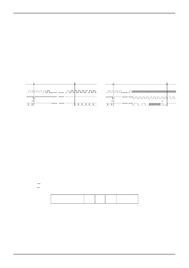
�?� The� BR24C21/F/FJ/FV� can� be� switched� from� Transmit-Only� Mode� to� Bi-directional� Mode� by� providing� a� valid� High� to� Low�
�transition� at� the� SCL� pin,� while� the� state� of� SDA� is� at� high-impedance.�
�?� After� a� valid� high� to� low� transition� on� the� SCL� pin,� the� BR24C21/F/FJ/FV� begins� to� count� the� VCLK� clock.� If� the� VCLK�
�counter� reaches� 128� clocks� without� the� command� for� Bi-directional� Mode,� the� device� reverts� to� Transmit-Only� Mode�
�(Recovery� function).� The� VCLK� counter� is� reset� by� providing� a� valid� high� to� low� transition� at� the� SCL� pin.� After� reversal� to�
�Transmit-Only� Mode� the� device� begins� to� output� data� (00h� address� data)� with� the� 129th� rising� clock� edge� of� VCLK.�
�?� If� the� BR24C21/F/FJ/FV� is� switched� from� Transmit-Only� Mode� and� receives� the� command� for� Bi-directional�
�Mode� and� responds� with� an� Acknowledge,� it� is� impossible� to� revert� to� Transmit-Only� Mode.� (Power� down�
�is� the� only�
�way� to� revert� to� Transmit-Only� Mode.)� Unless� the� input� device� code� is� “1010”,� the� device� does�
�not� respond� with� an�
�Acknowledge.� If� the� VCLK� counter� reaches� 128� clocks� afterwards,� it� is� possible� to� revert� to� Transmit-Only� Mode� for�
�Recovery� function.� If� the� Master� generates� a� STOP� condition� during� the� Slave� address,� before� an� Acknowledge� is� input,�
�it� is� possible� to� revert� to� Transmit-Only� Mode.�
�?� When� the� device� is� switched� from� Transmit-Only� Mode� to� Bi-direction� Mode,� the� period� of� tVHZ� needs� to� be� held.�
�t� o� r� return� to� Transmit-Only� Mode� -� O� n� l� y� M� o� d� e�
�t� return� to� Transmit-Only� Mode� i� t� -� O� n� l� y� M� o� d� e�
�Tra� nsm� it� -o� nl� y�
�MODE� Transmit-only�
�B� i� -� Bi-directional� l�
�d� e� w� ith� s� i�
�T� r� a� Transition� Mode� with� possibility� to� b� i� l� i� t� y�
�e� tu� ne� to� Tra� nsmit�
�Tra� nsm� it� -� On� l� y�
�Transmit-Only�
�MODE�
�Tra� nsm� it� -o� nl� y�
�Transmit-oOnly�
�Bi-directional� n� a� l�
�n� M� o� e� w� h�
�Transition� i� Mode� with� d� possibility� p� to� s� s� i� b� i� l� i� t� y�
�o� re� tu� ne� to� Tra� nsm�
�B� i� -� d� i� Bi-directional�
�p� a� r� m� parmanently�
�1�
�2�
�3�
�4�
�127� 128� 129�
�1�
�2�
�n<128�
�n�
�VCLK�
�VCLK�
�ADDRESS� 00h�
�SCL�
�tVHZ�
�ADDRESS� 00h�
�SCL�
�tVHZ�
�D7� D6� D5� D4�
�S�
�1�
�0�
�1�
�0�
�*�
�*�
�*� R/W� ACK�
�SDA�
�Figure� 6.� Recovery� Mode�
�SDA�
�Figure� 7.� Mode� Change�
�*� Don’t� care�
�○� Bi-directional� Mode�
�START� Condition�
�?� All� commands� are� proceeded� by� the� START� condition,� which� is� a� High� to� Low� transition� of� SDA� when� SCL� is� High.�
�?� The� BR24C21/F/FJ/FV� continuously� monitors� the� SDA� and� SCL� lines� for� the� START� condition� and� will� not� respond� to�
�any� commands� until� this� condition� has� been� met.�
�(See� Figure� 1� Synchronous� Data� Timing)�
�STOP� Condition�
�?� All� commands� must� be� terminated� by� a� STOP� condition,� which� is� a� Low� to� High� transition� of� SDA� when� SCL� is� High.�
�?� The� STOP� condition� causes� the� internal� write� cycle� to� write� data� into� the� memory� array� after� a� write� sequence.�
�?� The� STOP� condition� is� also� used� to� place� the� device� into� standby� power� mode� after� read� sequences.�
�?� A� STOP� condition� can� only� be� issued� after� the� transmitting� device� has� released� the� bus.�
�(See� Figure� 1� Synchronous� Data� Timing)�
�Device� Addressing�
�?� Following� the� START� condition,� the� Master� outputs� the� device� address� of� the� Slave� to� be� accessed.� The� most� significant�
�four� bits� of� Slave� address� are� the� “device� type� indentifier,”� For� the� BR24C21/F/FJ/FV� this� is� fixed� as� “1010.”�
�?� The� next� three� bits� of� the� slave� address� are� inconsequential.�
�?� The� last� bit� of� the� stream� determines� the� operation� to� be� performed.� When� set� to� “1”,� a� READ� operation� is� selected.�
�When� set� to� “0”,� a� WRITE� operation� is� initiated.�
�R/W� set� to� "0"� ?� ?� ?� ?� ?� ?� ?� ?� WRITE� (This� bit� is� also� set� to� "0"� for� random� read� operation)�
�R/W� set� to� "1"� ?� ?� ?� ?� ?� ?� ?� ?� READ�
�1010�
�*�
�*�
�*�
�_�
�R/W�
�*:� Don’t� care�
�○� Write� Protect� Function�
�?� Write� Enable� (VCLK)�
�When� using� the� BR24C21/F/FJ/FV� in� Bi-directional� Mode,� the� VCLK� pin� can� be� used� as� a� write� enable� pin.� Setting� VCLK�
�High� allows� normal� write� operations,� while� setting� VCLK� low� prevents� writing� to� any� location� in� the� array.�
�(See� Figure� 3� Write� Enable� Timing)�
�Changing� VCLK� from� High� to� Low� during� the� self-timed� program� operation� will� not� halt� programming� of� the� device.�
�www.rohm.com�
�?� 2012� ROHM� Co.,� Ltd.� All� rights� reserved.�
�TSZ22111� ?� 15� ?� 001�
�5/18�
�TSZ02201-0R2R0G100270-1-2�
�10.Jul.2012� Rev.001�
�相关PDF资料 |
PDF描述 |
|---|---|
| A3P250-1VQG100I | IC FPGA 1KB FLASH 250K 100-VQFP |
| AGM30DTMS-S189 | CONN EDGECARD 60POS R/A .156 SLD |
| AYM30DTBS-S189 | CONN EDGECARD 60POS R/A .156 SLD |
| ASM30DTBS-S189 | CONN EDGECARD 60POS R/A .156 SLD |
| AGM30DTBS-S189 | CONN EDGECARD 60POS R/A .156 SLD |
相关代理商/技术参数 |
参数描述 |
|---|---|
| BR24C21FV | 制造商:ROHM 制造商全称:Rohm 功能描述:EDID Memory (For display) |
| BR24C21FV-E2 | 功能描述:电可擦除可编程只读存储器 I2C 1K BIT 128 X 8 3.3V/5V 8PIN RoHS:否 制造商:Atmel 存储容量:2 Kbit 组织:256 B x 8 数据保留:100 yr 最大时钟频率:1000 KHz 最大工作电流:6 uA 工作电源电压:1.7 V to 5.5 V 最大工作温度:+ 85 C 安装风格:SMD/SMT 封装 / 箱体:SOIC-8 |
| BR24C32 | 制造商:未知厂家 制造商全称:未知厂家 功能描述:I2C Serial EEPROM |
| BR24C32A-10TU-1.8 | 功能描述:电可擦除可编程只读存储器 BUS SERIAL 电可擦除可编程只读存储器S RoHS:否 制造商:Atmel 存储容量:2 Kbit 组织:256 B x 8 数据保留:100 yr 最大时钟频率:1000 KHz 最大工作电流:6 uA 工作电源电压:1.7 V to 5.5 V 最大工作温度:+ 85 C 安装风格:SMD/SMT 封装 / 箱体:SOIC-8 |
| BR24C32A-10TU-2.7 | 功能描述:电可擦除可编程只读存储器 I2C 32K-BIT 4KX8 3.3V5V 8PIN RoHS:否 制造商:Atmel 存储容量:2 Kbit 组织:256 B x 8 数据保留:100 yr 最大时钟频率:1000 KHz 最大工作电流:6 uA 工作电源电压:1.7 V to 5.5 V 最大工作温度:+ 85 C 安装风格:SMD/SMT 封装 / 箱体:SOIC-8 |
发布紧急采购,3分钟左右您将得到回复。