参数资料
| 型号: | BR25L320FJ-WE2 |
| 厂商: | Rohm Semiconductor |
| 文件页数: | 15/17页 |
| 文件大小: | 0K |
| 描述: | IC EEPROM 32KBIT 5MHZ 8SOP |
| 标准包装: | 1 |
| 格式 - 存储器: | EEPROMs - 串行 |
| 存储器类型: | EEPROM |
| 存储容量: | 32K (4K x 8) |
| 速度: | 5MHz |
| 接口: | SPI 3 线串行 |
| 电源电压: | 1.8 V ~ 5.5 V |
| 工作温度: | -40°C ~ 85°C |
| 封装/外壳: | 8-SOIC(0.154",3.90mm 宽) |
| 供应商设备封装: | 8-SOP-J |
| 包装: | 标准包装 |
| 产品目录页面: | 1379 (CN2011-ZH PDF) |
| 其它名称: | BR25L320FJ-WE2DKR |
�� �
�
�BR25L010-W,� BR25L020-W,� BR25L040-W,� BR25L080-W,� BR25L160-W,� BR25L320-W,� BR25L640-W�
�Technical� Note�
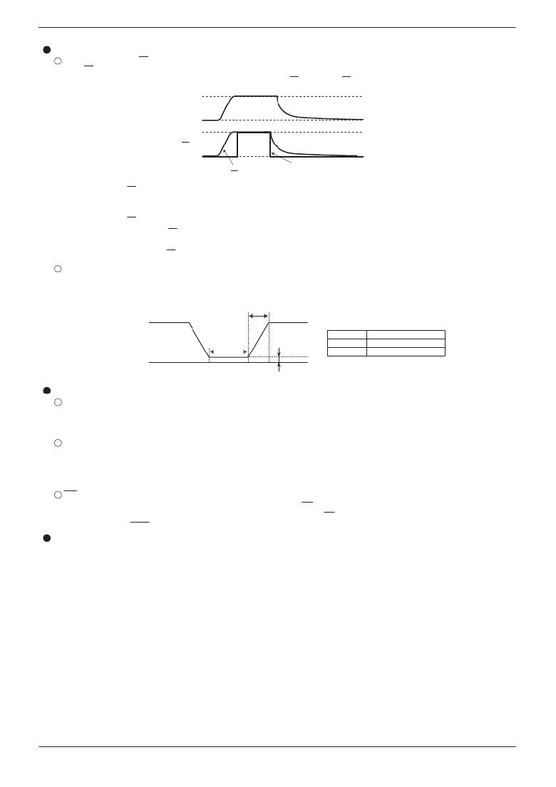
�Notes� on� power� ON/OFF�
�At� power� ON/OFF,� set� CS� "H"� (=� V� CC� ).�
�When� CS� is� "L",� this� IC� gets� in� input� accept� status� (active).� If� power� is� turned� on� in� this� status,� noises� and� the� likes� may� cause�
�malfunction,� mistake� write� or� so.� To� prevent� these,� at� power� ON,� set� CS� "H".� (When� CS� is� in� "H"� status,� all� inputs� are� canceled.)�
�Vcc�
�Vcc�
�GND�
�Vcc�
�CS�
�GND�
�Good� example�
�Bad� example�
�Fig.63� CS� timing� at� power� ON/OFF�
�(Good� example)�
�(Bad� example)�
�CS� terminal� is� pulled� up� to� V� CC� .�
�At� power� OFF,� take� 10ms� or� higher� before� re� supply.� If� power� is� turned� on� without� observing� this� condition,� the� IC� internal�
�circuit� may� not� be� reset,� which� please� note.�
�CS� terminal� is� "L"� at� power� ON/OFF.�
�In� this� case,� CS� always� becomes� "L"� (active� status),� and� EEPROM� may� have� malfunction,� mistake� write� owing� to� noises�
�and� the� likes.�
�Even� when� CS� input� is� High-Z,� the� status� becomes� like� this� case,� which� please� note.�
�PORcircuit�
�This� IC� has� a� POR� (Power� On� Reset)� circuit� as� mistake� write� countermeasure.� After� POR� action,� it� gets� in� write� disable� status.� The� POR�
�circuit� is� valid� only� when� power� is� ON,� and� does� not� work� when� power� is� OFF.� When� power� is� ON,� if� the� recommended� conditions� of� the�
�following� tR,� tOFF,� and� Vbot� are� not� satisfied,� it� may� become� write� enable� status� owing� to� noises� and� the� likes.�
�t� R�
�V� CC�
�Recommended� conditions� of� t� R� ,� t� OFF� ,� Vbot�
�t� R�
�t� OFF�
�Vbot�
�t� OFF�
�Vbot�
�10ms or below 10ms or higher 0.3V or below�
�100ms or below 10ms or higher 0.2V or below�
�0�
�Fig.64�
�Noise� countermeasures�
�Vcc� noise� (bypass� capacitor)�
�When� noise� or� surge� gets� in� the� power� source� line,� malfunction� may� occur,� therefore,� for� removing� these,� it� is� recommended� to� attach� a�
�by� pass� capacitor� (0.1� μ� F)� between� IC� Vcc� and� GND.� At� that� moment,� attach� it� as� close� to� IC� as� possible.�
�And,� it� is� also� recommended� to� attach� a� bypass� capacitor� between� board� Vcc� and� GND.�
�SCK� noise�
�When� the� rise� time� (tR)� of� SCK� is� long,� and� a� certain� degree� or� more� of� noise� exists,� malfunction� may� occur� owing� to� clock� bit� displacement.�
�To� avoid� this,� a� Schmitt� trigger� circuit� is� built� in� SCK� input.� The� hysteresis� width� of� this� circuit� is� set� about� 0.2V,� if� noises� exist� at� SCK� input,�
�set� the� noise� amplitude� 0.2Vp-p� or� below.� And� it� is� recommended� to� set� the� rise� time� (tR)� of� SCK� 100ns� or� below.� In� the� case� when� the� rise�
�time� is� 100ns� or� higher,� take� sufficient� noise� countermeasures.� Make� the� clock� rise,� fall� time� as� small� as� possible.�
�WP� noise�
�During� execution� of� write� status� register� command,� if� there� exist� noises� on� WP� pin,� mistake� in� recognition� may� occur� and� forcible� cancellation�
�may� result,� which� please� note.� To� avoid� this,� a� Schmitt� trigger� circuit� is� built� in� WP� input.� In� the� same� manner,� a� Schmitt� trigger� circuit� is�
�built� in� SI� input� and� HOLD� input� too.�
�Cautions� on� use�
�(1)� Described� numeric� values� and� data� are� design� representative� values,� and� the� values� are� not� guaranteed.�
�(2)� We� believe� that� application� circuit� examples� are� recommendable,� however,� in� actual� use,� confirm� characteristics� further� sufficiently.� In� the� case�
�of� use� by� changing� the� fixed� number� of� external� parts,� make� your� decision� with� sufficient� margin� in� consideration� of� static� characteristics�
�and� transition� characteristics� and� fluctuations� of� external� parts� and� our� LSI.�
�(3)� Absolute� maximum� ratings�
�If� the� absolute� maximum� ratings� such� as� impressed� voltage� and� operating� temperature� range� and� so� forth� are� exceeded,� LSI� may� be� destructed.�
�Do� not� impress� voltage� and� temperature� exceeding� the� absolute� maximum� ratings.� In� the� case� of� fear� exceeding� the� absolute� maximum�
�ratings,� take� physical� safety� countermeasures� such� as� fuses,� and� see� to� it� that� conditions� exceeding� the� absolute� maximum� ratings� should�
�not� be� impressed� to� LSI.�
�(4)� GND� electric� potential�
�Set� the� voltage� of� GND� terminal� lowest� at� any� action� condition.� Make� sure� that� each� terminal� voltage� is� lower� than� that� of� GND� terminal.�
�(5)� Heat� design�
�In� consideration� of� permissible� dissipation� in� actual� use� condition,� carry� out� heat� design� with� sufficient� margin.�
�(6)� Terminal� to� terminal� short� circuit� and� wrong� packaging�
�When� to� package� LSI� onto� a� board,� pay� sufficient� attention� to� LSI� direction� and� displacement.� Wrong� packaging� may� destruct� LSI.� And� in�
�the� case� of� short� circuit� between� LSI� terminals� and� terminals� and� power� source,� terminal� and� GND� owing� to� foreign� matter,� LSI� may� be�
�destructed.�
�(7)� Use� in� a� strong� electromagnetic� field� may� cause� malfunction,� therefore,� evaluate� design� sufficiently.�
�www.rohm.com�
�?� 2010� ROHM� Co.,� Ltd.� All� rights� reserved.�
�15/16�
�2010.07� -� Rev.� B�
�相关PDF资料 |
PDF描述 |
|---|---|
| RSM43DTBI-S189 | CONN EDGECARD 86POS R/A .156 SLD |
| RSM43DTMI-S189 | CONN EDGECARD 86POS R/A .156 SLD |
| RSM43DTAI-S189 | CONN EDGECARD 86POS R/A .156 SLD |
| RMM43DTBI-S189 | CONN EDGECARD 86POS R/A .156 SLD |
| RMM43DTMI-S189 | CONN EDGECARD 86POS R/A .156 SLD |
相关代理商/技术参数 |
参数描述 |
|---|---|
| BR25L320F-W | 制造商:ROHM 制造商全称:Rohm 功能描述:SPI BUS 32Kbit (4,096 x 8bit) EEPROM |
| BR25L320F-WE2 | 功能描述:电可擦除可编程只读存储器 SPI 32K BIT RoHS:否 制造商:Atmel 存储容量:2 Kbit 组织:256 B x 8 数据保留:100 yr 最大时钟频率:1000 KHz 最大工作电流:6 uA 工作电源电压:1.7 V to 5.5 V 最大工作温度:+ 85 C 安装风格:SMD/SMT 封装 / 箱体:SOIC-8 |
| BR25L320-W | 制造商:ROHM 制造商全称:Rohm 功能描述:SPI BUS Serial EEPROMs |
| BR25L640FJ-W | 制造商:ROHM 制造商全称:Rohm 功能描述:SPI BUS 64Kbit (8,192 x 8bit) EEPROM |
| BR25L640FJ-WE2 | 功能描述:电可擦除可编程只读存储器 SPI 8192X8 BIT RoHS:否 制造商:Atmel 存储容量:2 Kbit 组织:256 B x 8 数据保留:100 yr 最大时钟频率:1000 KHz 最大工作电流:6 uA 工作电源电压:1.7 V to 5.5 V 最大工作温度:+ 85 C 安装风格:SMD/SMT 封装 / 箱体:SOIC-8 |
发布紧急采购,3分钟左右您将得到回复。