- 您现在的位置:买卖IC网 > PDF目录295167 > BS616LV4020BC (BRILLIANCE SEMICONDUCTOR, INC.) Very Low Power/Voltage CMOS SRAM 256K x 16 or 512K x 8 bit switchable PDF资料下载
参数资料
| 型号: | BS616LV4020BC |
| 厂商: | BRILLIANCE SEMICONDUCTOR, INC. |
| 元件分类: | SRAM |
| 英文描述: | Very Low Power/Voltage CMOS SRAM 256K x 16 or 512K x 8 bit switchable |
| 中文描述: | 非常低功率/电压CMOS SRAM的256K × 16或512K × 8位开关 |
| 文件页数: | 2/8页 |
| 文件大小: | 255K |
| 代理商: | BS616LV4020BC |
Revision 2.1
Jan.
2004
2
R0201-BS616LV1611
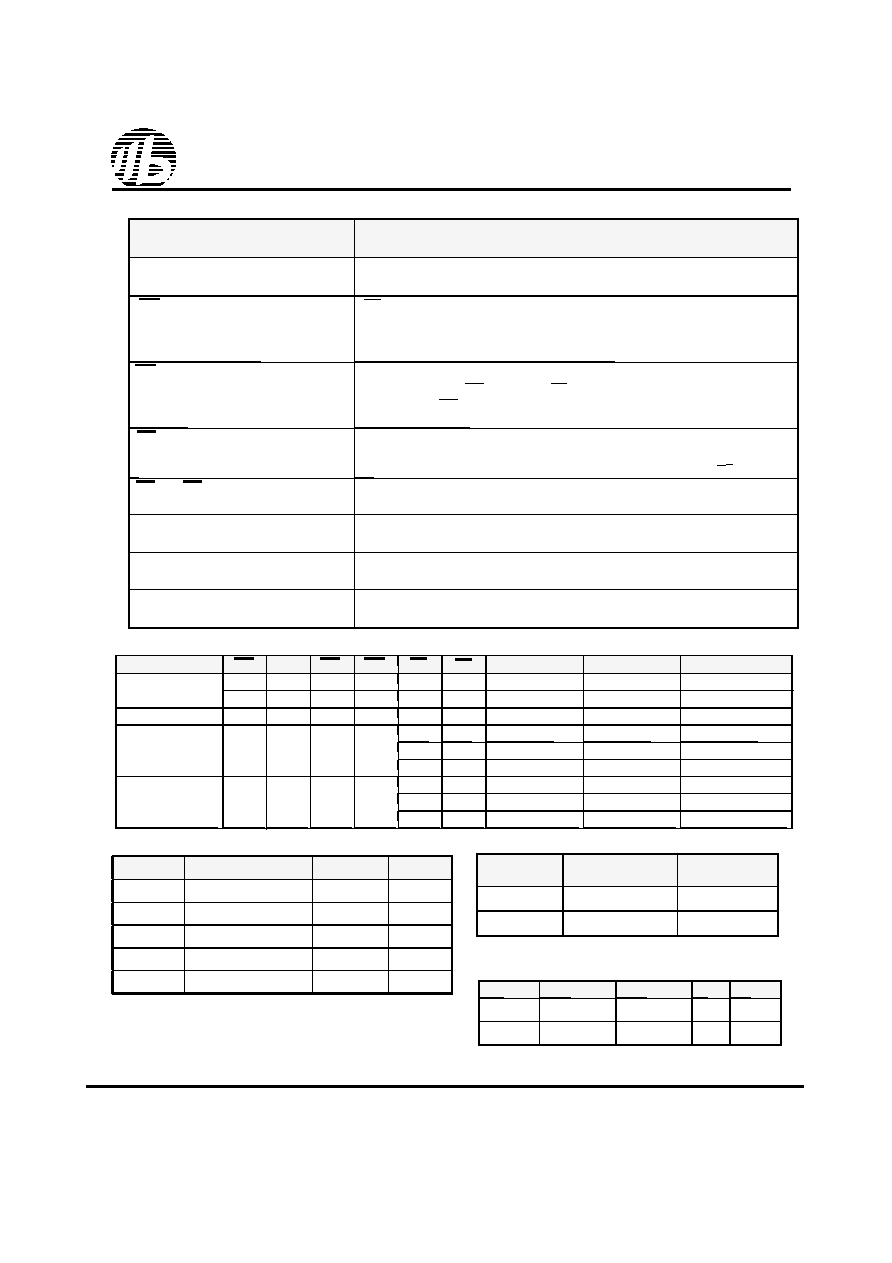
Name
Function
A0-A19 Address Input
These 20 address inputs select one of the 1,048,576 x 16-bit words in the RAM.
CE1 Chip Enable 1 Input
CE2 Chip Enable 2 Input
CE1 is active LOW and CE2 is active HIGH. Both chip enables must be active when
data read from or write to the device. If either chip enable is not active, the device is
deselected and is in a standby power mode. The DQ pins will be in the high
impedance state when the device is deselected.
WE Write Enable Input
The write enable input is active LOW and controls read and write operations. With the
chip selected, when WE is HIGH and OE is LOW, output data will be present on the
DQ pins; when WE is LOW, the data present on the DQ pins will be written into the
selected memory location.
OE Output Enable Input
The output enable input is active LOW. If the output enable is active while the chip is
selected and the write enable is inactive, data will be present on the DQ pins and they
will be enabled. The DQ pins will be in the high impedance state when OE is inactive.
LB and UB Data Byte Control Input
Lower byte and upper byte data input/output control pins.
D0 - D15 Data Input/Output Ports
These 16 bi-directional ports are used to read data from or write data into the RAM.
Vcc
Power Supply
Vss
Ground
TRUTH TABLE
PIN DESCRIPTIONS
BSI
BS616LV1611
MODE
CE1
CE2
WE
OE
LB
UB
D0~D7
D8~D15
Vcc CURRENT
H
X
High Z
ICCSB , ICCSB1
Not selected
(Power Down)
X
L
X
High Z
ICCSB , ICCSB1
Output Disabled
L
H
X
High Z
ICC
L
Dout
ICC
H
L
High Z
Dout
ICC
Read
L
H
L
H
Dout
High Z
ICC
LL
Din
ICC
HL
X
Din
ICC
Write
L
H
L
X
LH
Din
X
ICC
CIN
Input
Capacitance
VIN=0V
10
pF
CDQ
Input/Output
Capacitance
VI/O=0V
12
pF
RANGE
AMBIENT
TEMPERATURE
Vcc
Commercial
0
O C to +70O C
2.4V ~ 5.5V
Industrial
-40
O C to +85O C
2.4V ~ 5.5V
ABSOLUTE MAXIMUM RATINGS(1)
OPERATING RANGE
CAPACITANCE (1) (TA = 25oC, f = 1.0 MHz)
1. Stresses greater than those listed under ABSOLUTE MAXIMUM
RATINGS may cause permanent damage to the device. This is a
stress rating only and functional operation of the device at these
or any other conditions above those indicated in the operational
sections of this specification is not implied. Exposure to absolute
maximum rating conditions for extended periods may affect reliability.
1. This parameter is guaranteed and not 100% tested.
SYMBOL
PARAMETER
RATING
UNITS
VTERM
Terminal
Voltage
with
Respect to GND
-0.5 to
Vcc+0.5
V
TBIAS
Temperature Under Bias
-40 to +85
O C
TSTG
Storage Temperature
-60 to +150
O C
PT
Power Dissipation
1.0
W
IOUT
DC Output Current
20
mA
SYMBOL
PARAMETER
CONDITIONS
MAX.
UNIT
相关PDF资料 |
PDF描述 |
|---|---|
| BS616UV4020BC | Ultra Low Power/Voltage CMOS SRAM 256K x 16 or 512K x 8 bit switchable |
| BS616UV2019AC | Ultra Low Power/Voltage CMOS SRAM 128K X 16 bit |
| BS616UV2019ACP10 | Hex Buffer/Driver With Open-Drain Outputs 14-TVSOP -40 to 85 |
| BS616UV2019ACP85 | Hex Buffer/Driver With Open-Drain Outputs 14-TVSOP -40 to 85 |
| BS616UV2019AI | Hex Buffer/Driver With Open-Drain Outputs 14-TVSOP -40 to 85 |
相关代理商/技术参数 |
参数描述 |
|---|---|
| BS616LV4020BI | 制造商:BSI 制造商全称:Brilliance Semiconductor 功能描述:Very Low Power/Voltage CMOS SRAM 256K x 16 or 512K x 8 bit switchable |
| BS616LV4020DC | 制造商:BSI 制造商全称:Brilliance Semiconductor 功能描述:Very Low Power/Voltage CMOS SRAM 256K x 16 or 512K x 8 bit switchable |
| BS616LV4020DI | 制造商:BSI 制造商全称:Brilliance Semiconductor 功能描述:Very Low Power/Voltage CMOS SRAM 256K x 16 or 512K x 8 bit switchable |
| BS616LV4021 | 制造商:BSI 制造商全称:Brilliance Semiconductor 功能描述:Very Low Power/Voltage CMOS SRAM 256K x 16 or 512K x 8 bit switchable |
| BS616LV4021BC | 制造商:BSI 制造商全称:Brilliance Semiconductor 功能描述:Very Low Power/Voltage CMOS SRAM 256K x 16 or 512K x 8 bit switchable |
发布紧急采购,3分钟左右您将得到回复。